techmannih/nema34-mounted-stepper-controller
A USB-C PD-powered RP2040 motor controller with protected 48 V power, DRV8262 dual-bridge drive for a NEMA34 motor, regenerative-braking resistor, isolated sensing, hardware interlocks, and telemetry/status interfaces.
- Version
- 0.3.113
- License
- unset
- Stars
- 1
release/usb-pd-architecture.md
PCB

Schematic

# Power architecture and component review
Current design: RP2040, DRV8262DDVR, TPS26750, WAGO J2/J3, optional AS5600. This document replaces the obsolete STM32/TMC5160 description. The nine source schematic pages follow the signal and power paths below. Native electrical checks and physical qualification remain separate.
## Reference-board decision
The public sources retrieved on 2026-11-03 do **not** all use DATA-only MCU power:
| Reference | Observed MCU power path |
|---|---|
| [NEMA23 v1.4.7](https://tscircuit.com/imrishabh18/nema-23-stepper-controller) | `VFUSED -> U_PD_LOGIC AP63205 -> PD_LOGIC_5V -> D_PD_LOGIC -> VSYS`; the existing DATA diode also feeds VSYS. PWR or DATA can power logic. |
| [NEMA17 v1.0.48](https://tscircuit.com/imrishabh18/rp2040-motor-controller) | DATA powers the MCU. The published README explicitly requires DATA power for the PD-voltage alarm. |
| [NEMA14 RP2040 v1.13.2](https://tscircuit.com/AnasSarkiz/NEMA14_RP2040) | `PD_VBUS -> D_PD -> LOGIC_IN` and `DATA_VBUS -> D_DATA -> LOGIC_IN`; U_BUCK supplies V3V3. Both sources are supported. |
The user explicitly selected **DATA-only MCU power on 2026-11-05**. This now follows the NEMA17 power behaviour; the NEMA14/NEMA23 observations above remain historical reference facts. J10 must supply 5 V for RP2040 operation, including local START/STOP. J1 remains POWER-only. The 48 V EPR, independent motor-bus brake and hardware shutdown supplies remain separate. Exact reference release IDs and hashes are in `engineering/reviewer-power-reference.json`.
## Supplies and what each one powers
```mermaid
flowchart LR
J1["J1: PD POWER 5 V startup / 48 V EPR"] --> U5["U5 + L1: 3.3 V buck"]
J1 --> Protection["Q4/Q5 + U6: reverse block / eFuse"]
Protection --> VM["VMOTOR"]
VM --> U7["U7: integrated motor bridges"]
VM --> U22["U22 + L2: backup 3.3 V buck"]
U5 --> OR1["U23/U24: reverse-blocked selection"]
U22 --> OR1
OR1 --> Board["V3V3: sensing / logic / brake comparator"]
VM --> U34["U34 + L3: 12 V buck"]
U34 --> U15["U15: brake gate driver"]
Board --> Brake["U12/U13: independent brake threshold"]
Brake --> U15
U15 --> Q16["Q16 + J3 resistor: dissipate returned energy"]
OR2["U27: DATA-only reverse blocking"]
J10["J10: DATA 5 V"] --> U28["U28: current limit"]
U28 --> U25["U25: 3.3 V LDO"]
U25 --> OR2
OR2 --> MCU["V3V3_MCU: RP2040 + QSPI flash"]
```
U5, U22 and U34 are **LMR36510 step-down bucks**, not buck-boost converters. U25 is an LDO; U23/U24/U27 are ideal-diode devices, not voltage converters. J1 and J10 VBUS are never joined. U34 powers the **brake** gate driver, not DRV8262, which has its own charge pump.
| State | Intended electrical behaviour; bench verification still required |
|---|---|
| DATA only | RP2040 and its flash boot for USB recovery/diagnostics. Phase-current amplifiers and optional encoder are DATA-powered; board sensors, motor and brake rails are off. Power-off isolation prevents I2C back-feeding. |
| PD only | PD/protection logic is powered. RP2040, flash and encoder remain off; POWER_PERMIT and MCU_RUN pull-downs prevent motor enable. Local START/STOP is unavailable. |
| PD and DATA | DATA alone supplies MCU logic. U39 isolates the two I2C domains; U40 isolates board-status signals. No PD-to-MCU supply OR remains. |
| DATA removed while PD remains | MCU loses power; hardware pull-downs inhibit the motor. U39/U40 power-off isolation blocks board-side injection. Independent brake supplies remain active. Confirm real leakage, disable timing and no automatic restart on hardware. |
| PD removed while motor bus is charged or regenerating | U22 maintains comparator/control power from VMOTOR; U34 maintains brake gate power. The motor is inhibited, while the independent brake can dissipate energy. Backup availability and transient timing are not yet hardware-proven. |
Removing U22 without another motor-bus-powered brake-control path can disable the comparator while returned energy remains. Removing U34 disables the present Q16 gate-drive solution. A shared converter or a different brake switch is a separate power/thermal redesign, not a safe deletion to reduce a chip count.
## Isolation and startup contract
U26/R112/C77 and the board-to-MCU analog divider R119/R120 are removed. U27 is the sole MCU supply path, enabled by grounding CE. RP2040 GP28 reads `LOGIC_PG_MCU` digitally through U40; it no longer reports a board-voltage ADC value. U41 switches V3V3_MCU into V3V3_SENS for U31/U32 VS/REF2, U7 VCC, U42, the optional encoder and its pull-ups. All board-side I2C nets use the `_BOARD` suffix. U39 EN follows V3V3_MCU; the DATA-side 4.7 kΩ pull-ups cannot feed PD_3V3.
Verify PD-only, DATA-only, both-supply startup, DATA detach and PD loss with a meter/scope, including the unpowered rail. The buffer's Ioff rating is a bounded leakage specification, not proof of zero physical leakage. Reconnection must leave motion disarmed. The default diagnostic image keeps its four qualification locks false; explicit test profiles and their prerequisite records are described in [commissioning](commissioning.md).
The DATA-domain change also increases its active load. Each [INA240](https://www.ti.com/lit/ds/symlink/ina240.pdf) uses up to 2.6 mA over temperature (5.2 mA for the pair before MCU/flash/optional encoder). These amplifiers have no shutdown input, so U41 disconnects their supply during USB suspend. Stopping buses alone would leave that load powered. Total USB suspend current, including MCU, flash and regulator losses, still requires measurement before the compliance gate can close.
C22/C23 are now 1000 µF each. C18 is 1 µF to slow TPS26630 startup: the no-load nominal 48 V ramp is 0.96 s, about 0.10 A into the bulk capacitors. Load, MLCC bias and thermal regulation change this result. Verify actual startup completes within the eFuse timer and firmware sequencing; retain the driver inhibited throughout ramp.
## Driver variant decision
[TI DRV8262](https://www.ti.com/lit/ds/symlink/drv8262.pdf) specifies dual-bridge DDW at 5 A RMS and DDV at 10 A RMS (recommended operating conditions, SLVSFV5C section 5.3), subject to thermal design. DDW has its exposed thermal pad underneath; DDV has it on top, and the pin maps differ. They are not interchangeable on this PCB.
Retain **DRV8262DDVR** for the ordered 34HS31-6004S1 motor's 6 A/phase target. A cheaper DDWR could operate the motor at reduced current, but does not preserve that target. Neither the motor's phase label nor DDV's headline rating establishes an approved operating RMS current. The diagnostic image and the bounded test profiles are described in [commissioning](commissioning.md); see [thermal qualification](thermal-qualification.md). No supplier screenshot is treated as a current price/stock reservation.
## Every IC's purpose
| Ref | Device | Purpose and reason for retention |
|---|---|---|
| U1 | TPD4S480 | USB-C CC short-to-VBUS protection and EPR front-end control. Unused system-side SBU pins grounded as reviewed. |
| U2 | TPS26750 | Sink-only 48 V / 5 A EPR negotiation and power-path command; needs the verified U3 configuration. |
| U3 | M24512 | 64 KiB PD boot/configuration EEPROM; independent of MCU flash. |
| U4 | SN74LVC1G08 | AND of PD_PATH_OK and MCU POWER_PERMIT; prevents eFuse enable from either alone. |
| U5 | LMR36510 | PD input to 3.3 V, before the eFuse, so logic can boot before motor power is enabled. |
| U6 | TPS26630 | Input current limiting, undervoltage/overvoltage protection, fault latch and power-good indication. |
| U7 | DRV8262DDVR | Integrated dual H-bridge, current regulation, PH/EN and MCP4822 current references; top cooling remains unqualified. |
| U10 | SN74LVC1G08 | MCU_RUN AND physical MOTOR_PG. |
| U11 | SN74LVC1G08 | Adds independent VMOTOR_OK to the enable chain. |
| U12 | REF3425 | Stable 2.5 V reference for the brake and overvoltage comparators. |
| U13 | TLV3201 | Independent brake turn-on comparator near 52 V; works without a firmware brake command. |
| U14 | TLV3201 | Independent motor-overvoltage inhibit near 53.21 V. |
| U15 | UCC27511 | Drives Q16's gate from BRAKE_12V for controlled resistor switching. |
| U16 | RP2040 | USB diagnostics, PH/EN microstep sequencing, DAC commands and supervision; firmware qualification locks retained. |
| U17 | W25Q32JV, 4 MiB | RP2040 QSPI boot/program storage, powered on the MCU rail. |
| U18 | AS5600, DNP | Optional magnetic-angle telemetry. No validated rear magnet and no closed-loop motion claim. |
| U22 | LMR36510 | VMOTOR-derived 3.3 V backup for brake/control during PD loss. |
| U23 | LM66100 | Reverse-blocked PD-derived board-logic supply path. |
| U24 | LM66100 | Reverse-blocked motor-backup logic path; interlocked with U23. |
| U25 | TLV75533 | DATA-port 5 V to independent MCU 3.3 V. |
| U27 | LM66100 | DATA-derived supply path into the MCU rail, with reverse blocking. |
| U28 | TPS2553 | DATA-port overload current limiting; not a substitute for USB enumeration/suspend current compliance. |
| U29 | TMP102 | Board-temperature telemetry and TEMP_OK hardware inhibit. Board temperature is not driver junction temperature. |
| U30 | ADS1115 | Protected VMOTOR, input-current-monitor and brake-return ADC channels. |
| U31 | INA240A1 | Phase-A inline-shunt diagnostic amplifier. |
| U32 | INA240A1 | Phase-B inline-shunt diagnostic amplifier. Neither channel is the driver's current regulator. |
| U33 | SN74LVC1G08 | Adds TEMP_OK to RUN_WINDOW_OK, producing active-high RUN_SAFE. |
| U34 | LMR36510 | VMOTOR to 12 V for brake gate driver U15. Not a legacy external motor-bridge supply. |
| U35 | PCA9538 | I2C RGB and buzzer outputs. Hardware protection does not depend on the indicator bus. |
| U36 | SN74LVC2G66 | Isolates the PD controller's EEPROM bus for fixture programming. |
| U37 | SN74LVC1G17 | Reset-domain buffer for U35; protects the independent supply/reset relationship. |
| U38 | INA237 | Raw PD_VBUS ADC before the eFuse; 85 V bus capability, separate from VMOTOR measurement. |
| U39 | TCA9517A | Separates board PD I2C from DATA-powered MCU I2C; either rail off isolates the bus. Each side has its own pull-ups. |
| U40 | SN74LVC244A | DATA-powered, Ioff-capable buffer for six board-to-MCU status signals; unused inputs are grounded. Removes powered-board injection into an unpowered RP2040. |
| U41 | TPS22919 | Switches U7 VCC, U42, the phase-current amplifiers and optional encoder off during reset/suspend; QOD discharges V3V3_SENS. GP24 enables it only while peripheral operation is allowed. |
| U42 | MCP4822-E/SN | Dual 12-bit DAC supplies U7 VREF1/VREF2. SPI writes and simultaneous LDAC updates set phase-current magnitude; it has no readback. Powered from switched DATA-derived V3V3_SENS. |
## Enable equations and default states
`EFUSE_EN = PD_PATH_OK AND POWER_PERMIT`
`RUN_SAFE = MCU_RUN AND MOTOR_PG_BOARD AND VMOTOR_OK_BOARD AND TEMP_OK`
U4 is an input-power permission gate; U10/U11/U33 gate the motor driver. They are not four copies of the same function. Pull-downs hold the driver disabled and the permit inactive during reset. MCU fault handling remains additional to the hardware inhibit path. Consolidating gates into one package is possible only after checking placement, power domains, fault behaviour and rerouting; deleting gates or relying solely on software is not this review's solution.
PD_READY is a **derived firmware status**: fresh U38 conversion plus a live configured APP/sink/EPR 48 V / 5 A contract. MOTOR_PG is a separate physical eFuse signal. Stale ADC, sensor loss, invalid configuration, supply faults or an uncleared qualification gate prevent motion.
## Review and validation limits
Read the source-generated `release/schematics/*.svg` pages in order, with the component table and the two enable equations. The paired native KiCad schematic is currently a verification artifact: `normalize-kicad-parity.mjs` snaps its pin coordinates and assigns hidden net labels for parity/ERC. Use the visible source schematics for human circuit review; a zero-error native verification artifact is not proof of drawing readability. The DATA-only ECO changes the affected power domains, interfaces and local routing. Native/source parity and protection tests must be regenerated; a style-analysis pass alone does not prove human readability.
The eight known USB hole-clearance errors, cosmetic findings, unresolved sourcing, rear fastening, thermal/brake limits, actual programming/readback and powered tests remain visible. A readable schematic and a successful DRC run do not qualify the assembly.
### Sensor power and USB suspend
U41 (TPS22919DCKR, SC-70-6, JLC C2149796) switches DATA-derived `V3V3_MCU` into `V3V3_SENS` for U31/U32, U7 VCC, U42 and optional U18. GP24 `SENSE_EN` is active high; R145 holds it off during reset. QOD is connected to VOUT to discharge the rail when disabled. Firmware disables both phase enables, floats DAC SPI/LDAC and encoder I2C before power-off and waits 10 ms after enabling before accepting current/encoder readings. See the [TI pin table and output-discharge specification](https://www.ti.com/lit/ds/symlink/tps22919.pdf).
Suspend cancels the 50 kHz motion timer, disarms motion, ends peripheral buses, switches off U41 and uses alarm/WFE idle at 60 MHz. USB retains its 48 MHz clock. RP2040-E16 requires the system clock above 48 MHz while USB operates, so a 12 MHz system clock is inappropriate here. Resume restores the original system clock and timer; board readiness must settle again and motion remains disarmed. USB input current, resume timing and sensor-rail discharge still require measurement on the assembled board. This implementation is not USB compliance evidence.
Related Packages
 More from this authortechmannih/footprint-check-placementThis design features a 10mm x 10mm PCB with an integrated clock module chip connected to various digital, audio, and power nets, along with a nearby 100nF surface-mount capacitor for decoupling.
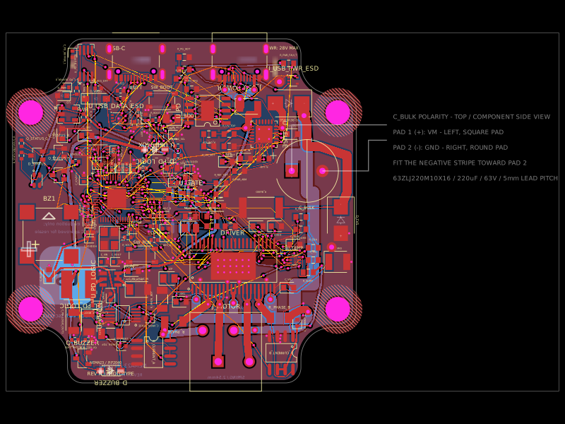 Similar packageimrishabh18/nema-23-stepper-controllerA 4-layer NEMA23 stepper-motor controller PCB combining an RP2040, DRV8462 dual-phase driver, USB-C Power Delivery/eFuse protection, current/voltage/temperature sensing, USB data multiplexing/ESD protection, optional AS5600 encoder, status LEDs, buzzer, and motor terminals.
 Discover something newabse/gameboy-advance