techmannih/nema34-mounted-stepper-controller
A USB-C PD-powered RP2040 motor controller with protected 48 V power, DRV8262 dual-bridge drive for a NEMA34 motor, regenerative-braking resistor, isolated sensing, hardware interlocks, and telemetry/status interfaces.
- Version
- 0.3.113
- License
- unset
- Stars
- 1
release/reviewer-power-reference.json
PCB

Schematic

{
"retrieved_at": "2026-11-03",
"method": "Public POST /package_releases/get by package_name, then /package_releases/get_filesystem_map by release ID. Original response files retained in local investigation output; selected raw file hashes below.",
"api": "https://api.tscircuit.com",
"references": [
{
"package": "imrishabh18/nema-23-stepper-controller",
"release_id": "f0035576-b40a-4016-b21d-ba222c8ae3bf",
"version": "1.4.7",
"release_url": "https://tscircuit.com/imrishabh18/nema-23-stepper-controller/releases/f0035576-b40a-4016-b21d-ba222c8ae3bf",
"files": {
"index.circuit.tsx": {
"sha256": "34e7d400a06d9c91299f619ac48202f1a480fd1f6c91ff4f403917cc13c64428",
"bytes": 9541
},
"usb-data-power.tsx": {
"sha256": "045d730133f8219349b9b2c6521c8dc7ccf15853075595250d08f307d3783b43",
"bytes": 7445
}
},
"observation": "PD VFUSED feeds AP63205 U_PD_LOGIC, then D_PD_LOGIC into VSYS; DATA also supplies VSYS."
},
{
"package": "imrishabh18/rp2040-motor-controller",
"release_id": "bc93e130-7357-4352-a45f-c9cf65563446",
"version": "1.0.48",
"release_url": "https://tscircuit.com/imrishabh18/rp2040-motor-controller/releases/bc93e130-7357-4352-a45f-c9cf65563446",
"files": {
"README.md": {
"sha256": "4acb242b6d0ce273f45d3acdda6819db6a64309040fc23897753b6a0d7fdd20a",
"bytes": 28039
},
"schematic/AutoLayoutSections.tsx": {
"sha256": "56683f3bb5954879ec4ffd34db79ec5fc3e3781b32c024971ce5ea85e3a9cffc",
"bytes": 5642
},
"schematic/ControllerSections.tsx": {
"sha256": "58a002ffb9150bc83fc061611754a778bea96c3a6bccdad2f2484d4dec237816",
"bytes": 454
}
},
"observation": "DATA supplies MCU; published README requires DATA for PD voltage alarm."
},
{
"package": "AnasSarkiz/NEMA14_RP2040",
"release_id": "09993ba5-47a4-4aa5-bc46-0791709b7698",
"version": "1.13.2",
"release_url": "https://tscircuit.com/AnasSarkiz/NEMA14_RP2040/releases/09993ba5-47a4-4aa5-bc46-0791709b7698",
"files": {
"index.circuit.json": {
"sha256": "7dd9884d5f4472dd4798d76333a2c22adf5cb5d5bb13fbf5097c928bbe795069",
"bytes": 5763737
},
"README.md": {
"sha256": "75e261d9c764d29e28e332e7255dbe9a1fbb42801f40d7abfd1ef2c1b6c963a4",
"bytes": 437
}
},
"observation": "D_PD and D_DATA cathodes join LOGIC_IN. U_BUCK VIN/EN use LOGIC_IN; FB and MCU IOVDD/VREG_IN use V3V3.",
"pin_net_evidence": {
"D_PD": [
{
"pin": 1,
"name": "cathode",
"net": "LOGIC_IN"
},
{
"pin": 2,
"name": "anode",
"net": "PD_VBUS"
}
],
"D_DATA": [
{
"pin": 1,
"name": "cathode",
"net": "LOGIC_IN"
},
{
"pin": 2,
"name": "anode",
"net": "DATA_VBUS"
}
],
"U_BUCK": [
{
"pin": 1,
"name": "FB",
"net": "V3V3"
},
{
"pin": 2,
"name": "EN",
"net": "LOGIC_IN"
},
{
"pin": 3,
"name": "VIN",
"net": "LOGIC_IN"
},
{
"pin": 4,
"name": "GND",
"net": "GND"
},
{
"pin": 5,
"name": "SW",
"net": "BUCK_SW"
},
{
"pin": 6,
"name": "BST",
"net": "BUCK_BST"
}
],
"U_MCU": [
{
"pin": 1,
"name": "IOVDD1",
"net": "V3V3"
},
{
"pin": 2,
"name": "GPIO0",
"net": null
},
{
"pin": 3,
"name": "GPIO1",
"net": null
},
{
"pin": 4,
"name": "GPIO2",
"net": "LED_G"
},
{
"pin": 5,
"name": "GPIO3",
"net": "LED_B"
},
{
"pin": 6,
"name": "GPIO4",
"net": null
},
{
"pin": 7,
"name": "GPIO5",
"net": null
},
{
"pin": 8,
"name": "GPIO6",
"net": "STEP"
},
{
"pin": 9,
"name": "GPIO7",
"net": "DIR"
},
{
"pin": 10,
"name": "IOVDD10",
"net": "V3V3"
},
{
"pin": 11,
"name": "GPIO8",
"net": "ENABLE_N"
},
{
"pin": 12,
"name": "GPIO9",
"net": "SLEEP"
},
{
"pin": 13,
"name": "GPIO10",
"net": "PD_GOOD"
},
{
"pin": 14,
"name": "GPIO11",
"net": null
},
{
"pin": 15,
"name": "GPIO12",
"net": null
},
{
"pin": 16,
"name": "GPIO13",
"net": null
},
{
"pin": 17,
"name": "GPIO14",
"net": null
},
{
"pin": 18,
"name": "GPIO15",
"net": null
},
{
"pin": 19,
"name": "TESTEN",
"net": "GND"
},
{
"pin": 20,
"name": "XIN",
"net": "XIN"
},
{
"pin": 21,
"name": "XOUT",
"net": "XOUT"
},
{
"pin": 22,
"name": "IOVDD22",
"net": "V3V3"
},
{
"pin": 23,
"name": "DVDD23",
"net": "V1V1"
},
{
"pin": 24,
"name": "SWCLK",
"net": "SWCLK"
},
{
"pin": 25,
"name": "SWDIO",
"net": "SWDIO"
},
{
"pin": 26,
"name": "RUN",
"net": "RUN"
},
{
"pin": 27,
"name": "GPIO16",
"net": "BUZZER_PWM"
},
{
"pin": 28,
"name": "GPIO17",
"net": null
},
{
"pin": 29,
"name": "GPIO18",
"net": null
},
{
"pin": 30,
"name": "GPIO19",
"net": null
},
{
"pin": 31,
"name": "GPIO20",
"net": null
},
{
"pin": 32,
"name": "GPIO21",
"net": null
},
{
"pin": 33,
"name": "IOVDD33",
"net": "V3V3"
},
{
"pin": 34,
"name": "GPIO22",
"net": null
},
{
"pin": 35,
"name": "GPIO23",
"net": null
},
{
"pin": 36,
"name": "GPIO24",
"net": null
},
{
"pin": 37,
"name": "GPIO25",
"net": "LED_R"
},
{
"pin": 38,
"name": "GPIO26",
"net": "TEMP_SDA"
},
{
"pin": 39,
"name": "GPIO27",
"net": "TEMP_SCL"
},
{
"pin": 40,
"name": "GPIO28",
"net": "VM_SENSE"
},
{
"pin": 41,
"name": "GPIO29",
"net": "DATA_PRESENT"
},
{
"pin": 42,
"name": "IOVDD42",
"net": "V3V3"
},
{
"pin": 43,
"name": "ADC_AVDD",
"net": "V3V3"
},
{
"pin": 44,
"name": "VREG_IN",
"net": "V3V3"
},
{
"pin": 45,
"name": "VREG_OUT",
"net": "V1V1"
},
{
"pin": 46,
"name": "USB_DM",
"net": "MCU_DM"
},
{
"pin": 47,
"name": "USB_DP",
"net": "MCU_DP"
},
{
"pin": 48,
"name": "USB_VDD",
"net": "V3V3"
},
{
"pin": 49,
"name": "IOVDD49",
"net": "V3V3"
},
{
"pin": 50,
"name": "DVDD50",
"net": "V1V1"
},
{
"pin": 51,
"name": "QSPI_SD3",
"net": "QSPI_SD3"
},
{
"pin": 52,
"name": "QSPI_SCLK",
"net": "QSPI_SCLK"
},
{
"pin": 53,
"name": "QSPI_SD0",
"net": "QSPI_SD0"
},
{
"pin": 54,
"name": "QSPI_SD2",
"net": "QSPI_SD2"
},
{
"pin": 55,
"name": "QSPI_SD1",
"net": "QSPI_SD1"
},
{
"pin": 56,
"name": "QSPI_SS",
"net": "QSPI_SS"
},
{
"pin": 57,
"name": "GND",
"net": "GND"
}
]
}
}
],
"decision": "Retain dual-source MCU behaviour seen in NEMA23 and NEMA14. Do not copy lower-voltage components or claim reference hardware qualification.",
"current_decision": {
"date": "2026-11-05",
"reason": "Explicit user selection supersedes dual-source reference choice",
"mcu_power": "DATA only; J10 required",
"references_unchanged": true
}
}
Related Packages
 More from this authortechmannih/footprint-check-placementThis design features a 10mm x 10mm PCB with an integrated clock module chip connected to various digital, audio, and power nets, along with a nearby 100nF surface-mount capacitor for decoupling.
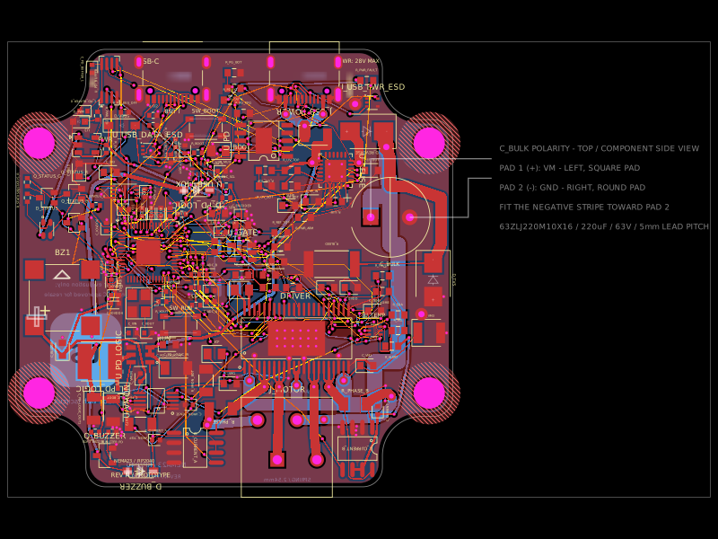 Similar packageimrishabh18/nema-23-stepper-controllerA 4-layer NEMA23 stepper-motor controller PCB combining an RP2040, DRV8462 dual-phase driver, USB-C Power Delivery/eFuse protection, current/voltage/temperature sensing, USB data multiplexing/ESD protection, optional AS5600 encoder, status LEDs, buzzer, and motor terminals.
 Discover something newabse/gameboy-advance