techmannih/nema34-mounted-stepper-controller
A USB-C PD-powered RP2040 motor controller with protected 48 V power, DRV8262 dual-bridge drive for a NEMA34 motor, regenerative-braking resistor, isolated sensing, hardware interlocks, and telemetry/status interfaces.
- Version
- 0.3.113
- License
- unset
- Stars
- 1
docs/source-design-rules.md
> The historical correction below predates the RP2040 redesign. Current rule values remain enforced, but current native proof is `docs/source-design-rules-check.json`; its board hash must match the delivered PCB. The old protected-geometry hash does not qualify the new architecture.

# Source/native design-rule correction — 2026-10-27

The current board additionally includes the [2026-10-28 parallel VMOTOR feed](copper-geometry-review.md). All rules below are unchanged and rechecked; the replay instructions here reconstruct the earlier rule correction, while the feed has its own main-952de54 baseline and replay command.

The previous main PCB did not implement all of the rules already declared in `index.circuit.tsx`. Its native project allowed 0.09 mm tracks; the native GND plane builder used 0.20 mm clearance. A passing report under those settings did not prove compliance with the source's requirements. This revision corrects the repository scripts and actual copper. It does not attribute those mismatches solely to the website's KiCad exporter.

| Constraint | Source, policy and delivered native PCB |
| --- | --- |
| Minimum routed track width | **0.15 mm**; every actual segment/arc is inspected, including copper inside pads |
| GND pour clearance | **0.30 mm**; both native GND zones use it |
| GND pour board-edge margin | **0.50 mm**; zone outlines are contained in the inward-offset board perimeter |
| Default inter-net routing clearance | **0.10 mm**, matching compiled source; this is independent of track width |
| Global copper-to-edge minimum | 0.20 mm; the stricter 0.50 mm inset applies specifically to GND pours |
| Connection/groove minimum | 0.09 mm, retained as a separate filled-copper check, not a track-width allowance |

The explicit values are recorded separately in `board-standards.json` and `hardware-contract.json`. The TSX declarations remain unchanged. `export-kicad-route.mjs`, `prepare-routing-rules.py` and `add-board-planes.py` derive the corresponding settings from this policy. Fresh export also reconstructs the GND inset from native Edge.Cuts with KiCad Python: the compiled polygon alone differed by 0.00329 mm² around its inset boundary. This native normalization is checked before export succeeds. The routing fingerprint now covers the policy and its generation helpers.

## Actual copper changes

The baseline contained 326 segments narrower than 0.15 mm. The correction widens or replaces those paths and adjusts adjacent copper to preserve clearance. Pad/footprint positions, component identities, logical nets, four mounting holes and schematic source remain unchanged. An exact reversible delta in `engineering/source-design-rule-eco.json` and the existing native ECO guard protect every unaffected native record; the historical protected hash is preserved.

The oscillator escape no longer squeezes a narrow track past U16's exposed pad. Its existing via moves outside the signal pad and the local route uses In2. One redundant GND via and dead-end/zero-length segments are removed. The larger GND clearance also required a local USB D− bottom-route change to maintain ground reference. No additional vias or components are introduced. The exact drill-over-solder-land audit finds the same 62 via-in-pad locations before/after; the earlier 63-location manufacturing inventory was stale. Its coordinates and documentation are refreshed. Filled/capped processing remains required.

The USB checker now derives each signal's own unavoidable antipad radius from its actual 0.50 mm via diameter plus the 0.30 mm GND clearance: 0.55 mm, with 0.001 mm polygon tolerance. It does not exempt gaps created by other nets. The unchanged route failed this check; the corrected route passes. Hardware clock startup, USB electrical compliance and thermal performance remain unmeasured.

## Evidence

- KiCad **10.0.5**, refilled zones, `--all-track-errors`, schematic parity: **0 errors, 0 unconnected items, 0 parity issues**. Schematic ERC: **0 violations**.
- **401 existing cosmetic warnings remain**: 189 text-height, 117 silk-over-copper and 95 silk-overlap findings. They are retained in the raw report; this is not a zero-total-violations board.
- `docs/source-design-rules-check.json` records actual track minimum, both GND clearances and zero outline area outside the required inset. Board, policy and checker hashes bind the evidence.
- Native Kelvin isolation, 44 bypass paths, buzzer bulk path, brake-divider removal and all four USB return-path checks pass on the delivered PCB.
- All 18 motor/supply/shunt/brake paths have fresh DC screens at 0.075 and 0.05 mm grids; the two unconverged cases were refined to 0.025 mm. Maximum before/after resistance increase is approximately **0.47%**, below the existing 5% regression limit. These are comparative calculations, not a current/thermal rating.
- Native filled-zone polygons match the exported Gerber conductor regions; detailed results are in `engineering/copper-geometry-review.json`.
- Replaying the hash-locked delta and refilling independently produces the same complete canonical PCB geometry, including fills, and the same native DRC counts.

## Reproduce and review

Run `bun run review` for the complete repository checks. The default source-rule check verifies hash-bound evidence and works without KiCad in GitHub Actions. To regenerate it locally, use KiCad's Python runtime:

```sh
KICAD_PYTHON=/path/to/kicad/python3 bun scripts/check-source-design-rules.mjs --refresh
```

That command also runs a native fixture which rejects a 0.09 mm track, 0.20 mm GND clearance and a plane reaching the board edge. Applying the correct GND policy cannot conceal the narrow track. Bun regression tests additionally reject source/native disagreement, stale evidence, altered ground zones and lost local routing.

For an independent reconstruction, extract both native PCB and project from commit `a58e277bcf781e29a529ddc8c464220ce60a4050`, retaining the original filename `pd1180-epr-r0.3`. Then run:

```sh
bun scripts/apply-source-rule-eco.mjs BASELINE/pd1180-epr-r0.3.kicad_pcb NEW_DIRECTORY
kicad-cli pcb drc --all-track-errors --refill-zones --save-board --severity-all --format json --output replay-drc.json NEW_DIRECTORY/pd1180-epr-r0.3.kicad_pcb
```

The replay refuses a different baseline or existing output directory. Open the delivered native project from `release/pd1180-epr-r0.3-kicad.zip` for source-matched schematic/PCB/rules. A fresh tscircuit.com KiCad download is a separate re-export and is not certified by this native-project result; the website exporter investigation remains separate.

Existing procurement, cosmetic manufacturing disposition, programming/readback, first-power, braking, thermal and mechanical qualification holds remain. Firmware motion locks are unchanged. This is an engineering review revision, not an order or motor-operation approval.
Related Packages
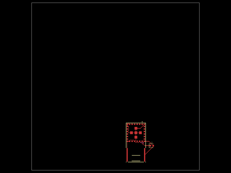 More from this authortechmannih/footprint-check-placementThis design features a 10mm x 10mm PCB with an integrated clock module chip connected to various digital, audio, and power nets, along with a nearby 100nF surface-mount capacitor for decoupling.
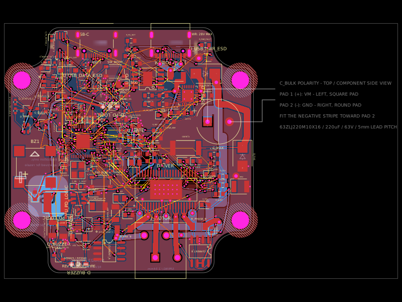 Similar packageimrishabh18/nema-23-stepper-controllerA 4-layer NEMA23 stepper-motor controller PCB combining an RP2040, DRV8462 dual-phase driver, USB-C Power Delivery/eFuse protection, current/voltage/temperature sensing, USB data multiplexing/ESD protection, optional AS5600 encoder, status LEDs, buzzer, and motor terminals.
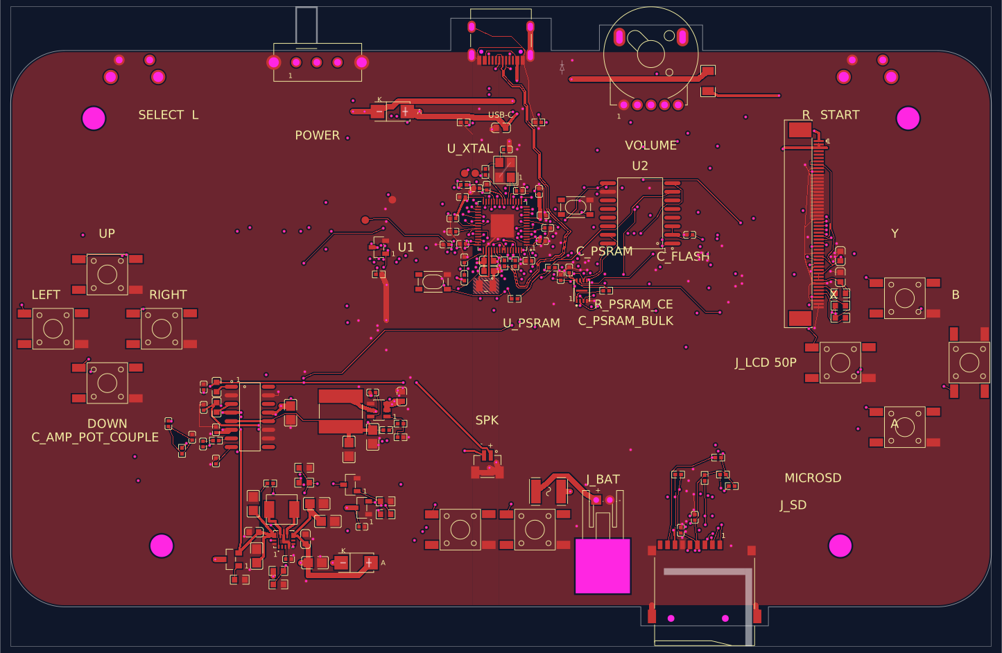 Discover something newabse/gameboy-advance