techmannih/nema34-mounted-stepper-controller
A USB-C PD-powered RP2040 motor controller with protected 48 V power, DRV8262 dual-bridge drive for a NEMA34 motor, regenerative-braking resistor, isolated sensing, hardware interlocks, and telemetry/status interfaces.
- Version
- 0.3.113
- License
- unset
- Stars
- 1
docs/rp2040-redesign.md
# RP2040 / DRV8262 redesign

Revision: 0.5.0-RP2040-DRAFT, architecture introduced from `1c22abf`, with the DATA-only MCU ECO based on merged main `fd77f02`. User-selected architecture: **RP2040 + DRV8262DDVR + TPS26750 + AS5600, retaining 48 V EPR**. This document describes the implemented architecture; [assembly](assembly.md) covers fabrication/installation and [commissioning](commissioning.md) covers measurements after assembly.

## Electrical changes

- U16 becomes RP2040 with its own 12 MHz ABM8-272-T3 crystal (CL 10 pF, 50 Ω ESR) with 15 pF load capacitors, 1 kΩ oscillator resistor, local I/O/core/VREG capacitors, QSPI boot wiring, 27 Ω USB series resistors and BOOTSEL test pad. Existing W25Q32JV U17 is now boot storage and is supplied from the independently powered MCU rail. TESTEN and exposed pad 57 are grounded. The compiled contract checks the package pins independently of the generated GPIO header.
- U7 becomes **DRV8262DDVR (DDV, 44 pins)**. It contains both motor H-bridges. Q6–Q13, Q14, the old gate networks and the TMC regulation shunts R109/R110 are removed. The DDW pinout/rating is not interchangeable. MODE1/MODE2 select dual PH/EN; U42 MCP4822 drives independent references, with 1.5k IPROPI resistors. Pins 31/35 remain NC.
- Motor nSLEEP is gated by RUN_SAFE independently of phase/DAC commands. The eFuse, thermal/voltage gates, brake Q16, freewheel clamp and brake-feedback monitor remain. U34 and L3 remain: their renamed BRAKE_12V output powers U15, even though the old TMC supply function is gone.
- R115/R116 and INA240 phase-current diagnostics remain; DRV8262 regulates using its internal current sensing. Their four Kelvin branches pass native terminal-only isolation and pour-keepout checks.
- U18 becomes AS5600, I²C address 0x36 on RP2040 I²C1. Its 5 V/3 V supply pins are tied to 3.3 V per the 3.3 V circuit, DIR is low, PGO is unconnected. It is **DNP**, centered on the motor axis on the bottom; both bypass capacitors stay on top. The single-shaft ordered motor has no qualified rear magnet installation. Firmware reports valid magnet/angle telemetry only, not closed-loop position control.
- J1/J10, PD controller/configuration, four mounting holes, brake attachment and other unrelated circuits are retained. The reviewer ECO replaces J2/J3 with WAGO spring clamps and adds U38 INA237 raw PD_VBUS sensing. ADS1115 still measures protected VMOTOR separately.

## DATA-only MCU power

U26 is removed. J10 → U28 → U25 → U27 supplies V3V3_MCU; the PD/motor rails retain independent protection/brake control. U39 isolates PD I²C, U40 isolates status lines, and U41 switches phase/encoder sensors off during USB suspend. Firmware stops the phase timer, disarms, and idles at 60 MHz to retain RP2040 USB clock requirements. Enumeration, USB current, sensor discharge and wake timing require hardware measurement.

## Firmware behavior

The new driver requires RP2040 PH/EN phase sequencing and U42 dual-DAC current references. The 20 µs scheduler advances 16 microsteps/full step, ramps to 10 rpm and limits the requested commissioning current to 0.8 A RMS. Nominal peak VREF is 359 mV; physical current requires calibration. The DAC has no readback. Default diagnostics inhibit motion; board-bound power/bench profiles implement stationary testing and a bounded 10-second run. Hardware RUN_SAFE gates nSLEEP independently of the sequencer.

A 25 ms command lease and late-timer fault stop pulses and lower enable. The fault latches rather than automatically restarting after a stalled loop. PD contract, eFuse power-good/fault, voltage window, temperature, brake continuity and driver-register checks remain required. The watchdog is serviced only by the main loop. No register OTP or AS5600 programming is performed.

USB-only startup retains boot-flash power. Firmware delays USB initialization until DATA VBUS is present and detaches when it disappears. Target tests cover initialization, detach/suspend/power-loss and timer-fault cases; USB current, enumeration, suspend current and GPIO timing remain **unmeasured**. See [firmware/README](../firmware/README.md) for RP2040 BOOTSEL/SWD programming and full-flash readback. The old STM32 image and address must not be used.

## Current and thermal limits

TI SLVSFV5C specifies up to 10 A RMS per bridge in the dual-bridge DDV package, subject to thermal limits. This is not a qualified continuous board current. At the separate 6 A RMS/phase analysis point, two-phase conduction `2 × Irms² × (RHS+RLS)` is 7.2 W with the 25 °C typical 0.100 Ω bridge resistance and 13.25 W with the 125 °C maximum 0.184 Ω case. Switching losses, waveform, airflow and the top-cooler/TIM stack require measurement. The selected cooler installation must be checked against the actual DDV exposed-top geometry.

Use the bounded current profile for initial tests and the selected driver/brake cooling parts in [thermal qualification](thermal-qualification.md). Record current, temperature and braking duty before selecting the application profile; 6 A/phase is the motor rating, not the test setting. The selected first-article external resistor is 10 Ω / 300 W with the specified case cooling.

TI section 9.1 requires support at both ends of the IC, recommends less than 45 N mounting force in production, and permits the heatsink to be grounded or floating. The DDV top junction-to-case resistance is 0.7 °C/W; heatsink and interface resistance must be added. Exact first-article cooler/TIM identities are selected in the thermal specification; physical end-support/contact geometry still needs a fitted installation, and the assembly CAD is not its fabrication drawing. Section 9.3 recommends 2 oz outer copper; this board's retained 1 oz stack has **not** been qualified as an equivalent thermal/current implementation. A heatsink picture or the IC's headline current rating cannot close these design requirements.

## Native CAD and verification

The current paired KiCad project has **0 unconnected items, 0 schematic-parity findings and 0 ERC findings**. Raw DRC retains **8 J1/J10 hole-clearance errors** at the user's explicit request, plus **488 cosmetic warnings** (191 text-height, 164 silkscreen overlaps and 133 silk-over-copper). This is not a zero-violation report or fabrication approval. No other native electrical/geometry finding is accepted.

The [KiCad GUI screenshot](drv8262-kicad-drc.png) records the DRV8262DDVR revision before the final source-owned R35/C97 reference alignment: 8 USB hole errors, 494 cosmetic warnings and 0 unconnected items. The final CLI run after that text-only correction reports 8 USB hole errors, 488 cosmetic warnings, zero unconnected/parity and zero ERC findings. GUI schematic parity was not enabled in the screenshot. `checks/drv8262-gui-evidence.json` identifies the photographed board; `engineering/copper-geometry-review.json` records the exact unchanged-copper comparison to the final board.

All 58 local bypass power paths, four terminal-only Kelvin branches, four USB return-plane paths, source/native width and ground-spacing rules, and power-corridor checks pass on the exported board. The USB fanout uses a filled/capped via in C103's pad; assembly must retain the documented filled/capped via-in-pad process. Final copper is imported into the routed viewer, rather than rerouted by the hosted preview. See [copper evidence](copper-geometry-review.md), [raw manufacturing report](../dist/manufacturing/manufacturing-report.json) and [generated full verification](verification.json).

The new DC-bus/brake/eFuse behavioral simulations are bound to this source. They do not model or qualify DRV8262 switching. The enlarged 2 × 1000 µF bank reaches **54.321 V** in the nominal-delay 6 A winding-corner screen, versus **54.858 V** for the previous 2 × 470 µF design. It passes the allocated 0.5 V reserve in that case; the 100 µs recovery screen still reaches **54.745 V** and fails that reserve. The 5 J stress also exceeds 55 V. Full-current operation remains unqualified. The low-current sensitivity case is separate and is not a guaranteed current-tolerance bound.

The manufacturing ZIP, BOM/CPL, Gerbers, drills, routed viewer and native reports are regenerated for this revision. The full `bun run review` result is recorded in `docs/verification.json`; the report identifies the checked revision and software/CAD results. Refresh exact quantities and arrange assembler allocation at ordering.

Remaining product/hardware work is recorded in [readiness](readiness.md): qualified DDV heatsink/TIM and motor-current envelope; secured rear mounting and optional magnet installation; physical validation of spring clamps and raw PD voltage sensing; the actual 48 V/5 A EPR source/cable and completed J3 brake installation; TI/RP2040 programming, full readback/cold boot, and staged powered fault/braking/thermal tests. No physical result is claimed.

## Primary references

- [TI DRV8262 datasheet](https://www.ti.com/lit/ds/symlink/drv8262.pdf): DDV pin table, recommended capacitors, PH/EN truth tables, IPROPI current scaling, thermal/layout data.
- [Raspberry Pi RP2040 datasheet](https://datasheets.raspberrypi.com/rp2040/rp2040-datasheet.pdf) and [hardware design guide](https://datasheets.raspberrypi.com/rp2040/hardware-design-with-rp2040.pdf): package pins, power, QSPI, crystal, USB, boot.
- [AS5600 manufacturer page](https://ams-osram.com/products/sensors/position-sensors/ams-as5600-position-sensor): 3.3 V circuit, I²C and magnet validity.
- [Ordered motor](https://www.omc-stepperonline.com/s-series-nema-34-stepper-motor-4-8nm-679-87oz-in-14mm-key-way-shaft-1m-cable-34hs31-6004s1): physical/rated motor, not measured controller performance.

## Reviewer ECO after PR #21

J2/J3 now use WAGO 2601-3104 and 236-402 spring clamps. U38 INA237 measures raw PD_VBUS before the eFuse, independently of ADS1115 VMOTOR. Firmware checks identity, configuration, fresh single-shot conversion completion and the 44–51 V engineering window before deriving PD_READY from the TPS contract. MOTOR_PG remains a separate hardware/firmware gate. See [completion handoff](completion-handoff.md) for diagnostics, exact wiring, physical acceptance and the motor STEP limitation.

### Analog current range

R146/R147 are 1.5 kΩ (C22843), giving nominal VREF = 0.318 V/A. At 6 A RMS sinusoidal phase current the peak reference would be approximately 2.698 V, within both the driver's 3.3 V reference limit and the 3.3 V DAC supply. This preserves headroom for later qualified current settings; it does not raise the present 800 mA firmware ceiling. At that ceiling the nominal peak reference is 359 mV. The driver's minimum specified reference is 50 mV, so the sequencer brakes a winding below that value rather than claiming accurate near-zero regulation.

Phase B enable uses RP2040 GP13 (package pin 16), reusing the former HOME-input pad escape. GP4 (pin 6) is NC. The source pin contract and generated firmware header bind this assignment; no board-to-MCU buffer output remains attached to GP13.

The previous DRV8462 GUI capture is retained unchanged in [the historical evidence archive](kicad-drc-history.zip), keeping duplicate image data outside the hosted GitHub import payload.
Related Packages
 More from this authortechmannih/footprint-check-placementThis design features a 10mm x 10mm PCB with an integrated clock module chip connected to various digital, audio, and power nets, along with a nearby 100nF surface-mount capacitor for decoupling.
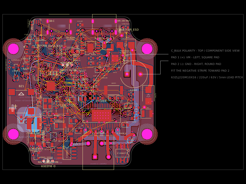 Similar packageimrishabh18/nema-23-stepper-controllerA 4-layer NEMA23 stepper-motor controller PCB combining an RP2040, DRV8462 dual-phase driver, USB-C Power Delivery/eFuse protection, current/voltage/temperature sensing, USB data multiplexing/ESD protection, optional AS5600 encoder, status LEDs, buzzer, and motor terminals.
 Discover something newabse/gameboy-advance