shibosoftwaredev/f1c100s-linux-nema8-stepper-controller
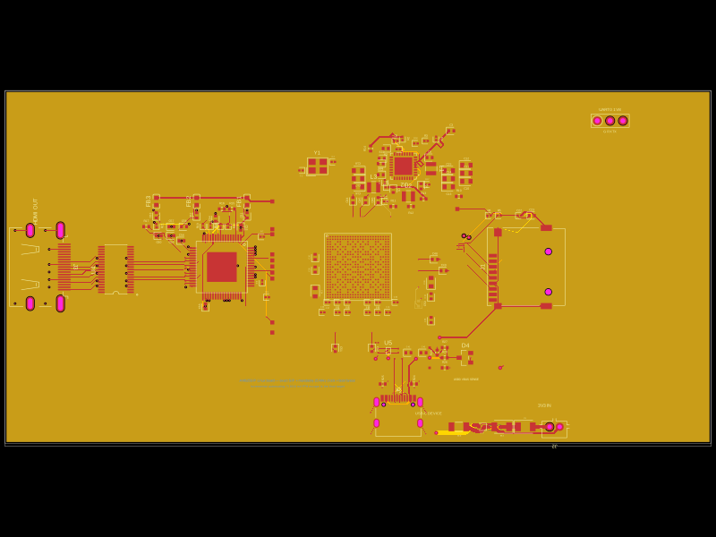
Restores component part numbers and CAD models, removes test-point 3D bodies, and validates that solder paste exists only on top-side SMT pads without altering copper or DRC.
- Version
- 0.3.5
- License
- unset
- Stars
- 0
motor-stage.tsx
import { B4B_PH_K_S_LF__SN_ } from "./imports/B4B_PH_K_S_LF__SN_"
import { DRV8825PWPR } from "./imports/DRV8825PWPR"
import { HoLRT1206_1W_300mR_1_ } from "./imports/HoLRT1206_1W_300mR_1_"
import { PMEG6020ELRX } from "./imports/PMEG6020ELRX"
import { TCJD226M050R0090E } from "./imports/TCJD226M050R0090E"
import { TMP102AIDRLR } from "./imports/TMP102AIDRLR"

const signal = { thickness: 0.15 } as const
const ground = { thickness: 0.3 } as const
const power = { thickness: 0.8 } as const
// Request 0.30 mm phase copper; the router may neck locally at the driver's
// 0.65 mm-pitch pins. The protected motor-input path uses 0.80 mm copper.
const motor = { thickness: 0.3 } as const

const connect = (name: string, from: string, to: string, thickness = 0.15) =>
  <trace name={name} from={from} to={to} thickness={thickness} />

/**
 * A 15 V USB-PD, 0.58 A-peak stage for StepperOnline 8HS15-0604S NEMA 8.
 * A dedicated STM32 generates STEP/DIR. The enable line drives nRESET and
 * nSLEEP and is pulled down, so the bridge cannot energize during either CPU's
 * reset or before the USB-PD power-good interlock closes.
 */
export function MotorStage() {
  return <group name="MOTOR_STAGE" pcbX={5} pcbY={0} schX={-35} schY={0} schSheetName="motion">
    <net name="VMOTOR" nominalTraceWidth={0.8} />
    <net name="DRV_VREF" nominalTraceWidth={0.15} />

    <fuse name="F_VM" currentRating="2A" voltageRating="30V" footprint="1812"
      supplierPartNumbers={{jlcpcb:["C960026"]}} manufacturerPartNumber="BSMD1812-200-30V"
      pcbX={27.3} pcbY={11.3} schX={46} schY={12} />
    <PMEG6020ELRX name="D_VM_BLOCK" pcbX={33} pcbY={11.2} pcbRotation={180} schX={49} schY={12} />
    <chip name="D_VM_TVS" footprint="smb" pcbX={40} pcbY={12.2} pcbRotation={180}
      pinLabels={{pin1:"TVS1",pin2:"TVS2"}}
      supplierPartNumbers={{jlcpcb:["C1975329"]}} manufacturerPartNumber="SMBJ22CAQ-13-F"
      schX={49} schY={8} schRotation={90} />
    <TCJD226M050R0090E name="C_VM_BULK" pcbX={42} pcbY={2} pcbRotation={90}
      schX={52} schY={8} schOrientation="vertical" />
    <capacitor name="C_VM_CER" capacitance="10uF" maxVoltageRating="50V" footprint="1206"
      supplierPartNumbers={{jlcpcb:["C13585"]}} manufacturerPartNumber="CL31A106KBHNNNE"
      pcbX={34} pcbY={8.5} schX={55} schY={8} schOrientation="vertical"
      maxDecouplingTraceLength={30} />

    <DRV8825PWPR name="U_MOTOR" noConnect={["DECAY","nHOME","NC"]}
      pcbX={34} pcbY={0} pcbRotation={0} schX={43} schY={0} schWidth={7} schHeight={9}
      schPinArrangement={{
        leftSide:{pins:[22,20,16,17,18,21,24,25,26],direction:"top-to-bottom"},
        rightSide:{pins:[5,7,10,8,6,9,19,27,23],direction:"top-to-bottom"},
        topSide:{pins:[4,11,1,2,3,15],direction:"left-to-right"},
        bottomSide:{pins:[12,13,14,28,29],direction:"left-to-right"},
      }} />

    {/* Charge pump, motor-rail bypassing, current regulation and safe defaults. */}
    <capacitor name="C_CP" capacitance="10nF" maxVoltageRating="50V" footprint="0402"
      supplierPartNumbers={{jlcpcb:["C15195"]}} pcbX={28.5} pcbY={-4.7} schX={39} schY={6} maxDecouplingTraceLength={25} />
    <capacitor name="C_VCP" capacitance="100nF" maxVoltageRating="50V" footprint="0402"
      supplierPartNumbers={{jlcpcb:["C960916"]}} pcbX={27} pcbY={-2.8} schX={42} schY={6} maxDecouplingTraceLength={25} />
    <resistor name="R_VCP" resistance="1M" footprint="0402"
      supplierPartNumbers={{jlcpcb:["C26083"]}} pcbX={26} pcbY={-5} schX={45} schY={6} />
    <capacitor name="C_VMA" capacitance="100nF" maxVoltageRating="50V" footprint="0402"
      supplierPartNumbers={{jlcpcb:["C960916"]}} pcbX={30.5} pcbY={-4.8} schX={48} schY={6} maxDecouplingTraceLength={25} />
    <capacitor name="C_VMB" capacitance="100nF" maxVoltageRating="50V" footprint="0402"
      supplierPartNumbers={{jlcpcb:["C960916"]}} pcbX={36.5} pcbY={-4.8} schX={51} schY={6} maxDecouplingTraceLength={25} />
    <capacitor name="C_DRV_3V3" capacitance="470nF" maxVoltageRating="16V" footprint="0402"
      supplierPartNumbers={{jlcpcb:["C480644"]}} pcbX={40.5} pcbY={-4} schX={39} schY={-7} maxDecouplingTraceLength={25} />
    <resistor name="R_REF_TOP" resistance="5.6k" footprint="0402"
      supplierPartNumbers={{jlcpcb:["C25908"]}} pcbX={38} pcbY={7} schX={42} schY={-7} />
    <resistor name="R_REF_BOTTOM" resistance="2k" footprint="0402"
      supplierPartNumbers={{jlcpcb:["C4109"]}} pcbX={34} pcbY={5} schX={45} schY={-7} />
    <capacitor name="C_REF" capacitance="100nF" maxVoltageRating="16V" footprint="0402"
      supplierPartNumbers={{jlcpcb:["C1525"]}} pcbX={32} pcbY={5} schX={48} schY={-7} maxDecouplingTraceLength={25} />
    <resistor name="R_ENABLE_PD" resistance="100k" footprint="0402"
      supplierPartNumbers={{jlcpcb:["C25741"]}} pcbX={27.5} pcbY={0} schX={37} schY={-3} />
    <resistor name="R_FAULT_PU" resistance="10k" footprint="0402"
      supplierPartNumbers={{jlcpcb:["C25744"]}} pcbX={40} pcbY={8} schX={37} schY={-5} />
    <HoLRT1206_1W_300mR_1_ name="R_ISEN_A" pcbX={30.5} pcbY={-7.5}
      schX={51} schY={-4} schOrientation="vertical" />
    <HoLRT1206_1W_300mR_1_ name="R_ISEN_B" pcbX={37.5} pcbY={-7.5}
      schX={54} schY={-4} schOrientation="vertical" />

    <B4B_PH_K_S_LF__SN_ name="J_MOTOR" pcbX={34} pcbY={-20.5} pcbRotation={0}
      schX={55} schY={0} />

    {/* TMP102 measures the driver-area board temperature; ALERT is read by PE6. */}
    <TMP102AIDRLR name="U_TEMP" pcbX={30} pcbY={-10.2} pcbRotation={0}
      schX={43} schY={-10.5} />
    <capacitor name="C_TEMP" capacitance="100nF" maxVoltageRating="16V" footprint="0402"
      supplierPartNumbers={{jlcpcb:["C1525"]}} pcbX={27.5} pcbY={-10.2}
      schX={47} schY={-10.5} schOrientation="vertical" maxDecouplingTraceLength={25} />
    <resistor name="R_TEMP_ALERT" resistance="10k" footprint="0402"
      supplierPartNumbers={{jlcpcb:["C25744"]}} pcbX={30} pcbY={-12.2}
      schX={39} schY={-10.5} schOrientation="vertical" />

    {/* USB-PD input protection and local motor-energy storage. */}
    {connect("VM_INPUT", "net.VBUS_PD", ".F_VM > .pin1", 0.8)}
    <trace name="VM_FUSED" from=".F_VM > .pin2" to=".D_VM_BLOCK > .anode"
      thickness={power.thickness} pcbStraightLine />
    {connect("VM_PROTECTED", ".D_VM_BLOCK > .cathode", "net.VMOTOR", power.thickness)}
    {connect("VM_TVS", ".D_VM_TVS > .pin1", "net.VMOTOR", 0.8)}
    {connect("VM_TVS_GND", ".D_VM_TVS > .pin2", "net.BOARD_GND", 0.8)}
    {connect("VM_BULK", ".C_VM_BULK > .pin1", "net.VMOTOR", 0.8)}
    {connect("VM_BULK_GND", ".C_VM_BULK > .pin2", "net.BOARD_GND", 0.8)}
    {connect("VM_CER", ".C_VM_CER > .pin1", "net.VMOTOR", 0.8)}
    {connect("VM_CER_GND", ".C_VM_CER > .pin2", "net.BOARD_GND", 0.8)}

    {/* DRV8825 supply and charge pump. */}
    {connect("DRV_VMA", ".U_MOTOR > .VMA", "net.VMOTOR", 0.8)}
    {connect("DRV_VMB", ".U_MOTOR > .VMB", "net.VMOTOR", 0.8)}
    {connect("DRV_C_VMA", ".C_VMA > .pin1", ".U_MOTOR > .VMA", 0.12)}
    {connect("DRV_C_VMA_GND", ".C_VMA > .pin2", "net.BOARD_GND", 0.3)}
    {connect("DRV_C_VMB", ".C_VMB > .pin1", ".U_MOTOR > .VMB", 0.12)}
    {connect("DRV_C_VMB_GND", ".C_VMB > .pin2", "net.BOARD_GND", 0.3)}
    {connect("DRV_CP1", ".U_MOTOR > .CP1", ".C_CP > .pin1")}
    {connect("DRV_CP2", ".U_MOTOR > .CP2", ".C_CP > .pin2")}
    {connect("DRV_VCP", ".U_MOTOR > .VCP", ".C_VCP > .pin1", 0.12)}
    {connect("DRV_VCP_RETURN", ".C_VCP > .pin2", "net.VMOTOR")}
    {connect("DRV_VCP_PULL", ".R_VCP > .pin1", ".U_MOTOR > .VCP", 0.12)}
    {connect("DRV_VCP_PULL_RETURN", ".R_VCP > .pin2", "net.VMOTOR")}

    {/* 0.58 A peak/phase: 0.868 V reference and 0.30 ohm sense resistors. */}
    {connect("DRV_3V3_BYPASS", ".U_MOTOR > .V3P3OUT", ".C_DRV_3V3 > .pin1", 0.12)}
    {connect("DRV_3V3_GND", ".C_DRV_3V3 > .pin2", "net.BOARD_GND")}
    {connect("DRV_REF_FEED", ".U_MOTOR > .V3P3OUT", ".R_REF_TOP > .pin1", 0.12)}
    {connect("DRV_REF_DIV", ".R_REF_TOP > .pin2", "net.DRV_VREF")}
    {connect("DRV_REF_BOTTOM", ".R_REF_BOTTOM > .pin1", "net.DRV_VREF")}
    {connect("DRV_REF_GND", ".R_REF_BOTTOM > .pin2", "net.BOARD_GND")}
    {connect("DRV_REF_CAP", ".C_REF > .pin1", "net.DRV_VREF")}
    {connect("DRV_REF_CAP_GND", ".C_REF > .pin2", "net.BOARD_GND")}
    {connect("DRV_AVREF", ".U_MOTOR > .AVREF", "net.DRV_VREF")}
    {connect("DRV_BVREF", ".U_MOTOR > .BVREF", "net.DRV_VREF")}
    {connect("DRV_ISEN_A", ".U_MOTOR > .ISENA", ".R_ISEN_A > .pin1", 0.12)}
    {connect("DRV_ISEN_A_GND", ".R_ISEN_A > .pin2", "net.BOARD_GND", 0.4)}
    {connect("DRV_ISEN_B", ".U_MOTOR > .ISENB", ".R_ISEN_B > .pin1", 0.12)}
    {connect("DRV_ISEN_B_GND", ".R_ISEN_B > .pin2", "net.BOARD_GND", 0.4)}

    {/* Dedicated motion-MCU control. 1/16 microstep mode is fixed in hardware. */}
    {connect("TRACE_MOTOR_STEP", ".U_MOTOR > .STEP", "net.MOTOR_STEP")}
    {connect("TRACE_MOTOR_DIR", ".U_MOTOR > .DIR", "net.MOTOR_DIR")}
    {connect("MOTOR_SLEEP", ".U_MOTOR > .nSLEEP", "net.MOTOR_ENABLE")}
    {connect("MOTOR_RESET", ".U_MOTOR > .nRESET", "net.MOTOR_ENABLE")}
    {connect("MOTOR_ENABLE_PULLDOWN", ".R_ENABLE_PD > .pin1", "net.MOTOR_ENABLE")}
    {connect("MOTOR_ENABLE_PULLDOWN_GND", ".R_ENABLE_PD > .pin2", "net.BOARD_GND")}
    <trace name="TRACE_MOTOR_FAULT" from=".U_MOTOR > .nFAULT" to=".R_FAULT_PU > .pin1"
      thickness={signal.thickness}
      pcbPath={[".U_MOTOR > .nFAULT", {x:2.275,y:5.5}, {x:5.49,y:5.5}, ".R_FAULT_PU > .pin1"]} />
    {connect("MOTOR_FAULT_PULLUP", ".R_FAULT_PU > .pin1", "net.MOTOR_FAULT")}
    {connect("MOTOR_FAULT_PULLUP_3V3", ".R_FAULT_PU > .pin2", "net.V3V3")}
    <trace name="DRV_ENABLE_ACTIVE" from=".U_MOTOR > .nENBL" to=".U_MOTOR > .pin29"
      pcbPath={[".U_MOTOR > .nENBL",{x:0.325,y:1.4},{x:0,y:1.4},".U_MOTOR > .pin29"]} />
    <trace name="DRV_MODE0" from=".U_MOTOR > .MODE0" to=".U_MOTOR > .pin29"
      pcbPath={[".U_MOTOR > .MODE0",{x:-1.625,y:1.4},{x:0,y:1.4},".U_MOTOR > .pin29"]} />
    <trace name="DRV_MODE1" from=".U_MOTOR > .MODE1" to=".U_MOTOR > .pin29"
      pcbPath={[".U_MOTOR > .MODE1",{x:-2.275,y:1.4},{x:0,y:1.4},".U_MOTOR > .pin29"]} />
    {connect("DRV_MODE2", ".U_MOTOR > .MODE2", "net.V3V3", 0.12)}
    {connect("DRV_GND1", ".U_MOTOR > .GND1", "net.BOARD_GND", 0.3)}
    {connect("DRV_GND2", ".U_MOTOR > .GND2", "net.BOARD_GND", 0.3)}
    {connect("DRV_EP_GND", ".U_MOTOR > .EP", "net.BOARD_GND", 0.8)}

    {/* Motor phases. */}
    {connect("MOTOR_A_PLUS", ".U_MOTOR > .AOUT1", ".J_MOTOR > .pin1", motor.thickness)}
    {connect("MOTOR_A_MINUS", ".U_MOTOR > .AOUT2", ".J_MOTOR > .pin2", motor.thickness)}
    <trace name="MOTOR_B_PLUS" from=".U_MOTOR > .BOUT1" to=".J_MOTOR > .pin3" thickness={motor.thickness}
      pcbPath={[".U_MOTOR > .BOUT1",
        {x:1.625,y:-4}, {x:1.1,y:-4.4},
        {x:1.1,y:-5.4}, {x:1.1,y:-5.4,via:true,fromLayer:"top",toLayer:"bottom"}, {x:1.1,y:-5.4},
        {x:5,y:-6}, {x:5,y:-17}, ".J_MOTOR > .pin3"]} />
    <trace name="MOTOR_B_MINUS" from=".U_MOTOR > .BOUT2" to=".J_MOTOR > .pin4" thickness={motor.thickness}
      pcbPath={[".U_MOTOR > .BOUT2",
        {x:0.325,y:-5}, {x:0.325,y:-5,via:true,fromLayer:"top",toLayer:"inner2"}, {x:0.325,y:-5},
        {x:-0.5,y:-6.2}, {x:0.8,y:-7.5}, {x:0.8,y:-17}, ".J_MOTOR > .pin4"]} />

    {/* Temperature monitor on the dedicated motion MCU's I2C bus. */}
    {connect("TEMP_VDD", ".U_TEMP > .V_POS", "net.V3V3")}
    {connect("TEMP_GND", ".U_TEMP > .GND", "net.BOARD_GND", 0.3)}
    {connect("TEMP_ADDR", ".U_TEMP > .ADD0", ".C_TEMP > .pin2", 0.12)}
    {connect("TEMP_SDA", ".U_TEMP > .SDA", "net.MOTION_I2C_SDA")}
    {connect("TEMP_SCL", ".U_TEMP > .SCL", "net.MOTION_I2C_SCL")}
    {connect("TEMP_ALERT", ".U_TEMP > .ALERT", "net.MOTION_TEMP_ALERT")}
    {connect("TEMP_ALERT_PULLUP", ".R_TEMP_ALERT > .pin1", "net.MOTION_TEMP_ALERT")}
    {connect("TEMP_ALERT_PULLUP_3V3", ".R_TEMP_ALERT > .pin2", "net.V3V3")}
    {connect("TEMP_BYPASS", ".C_TEMP > .pin1", ".U_TEMP > .V_POS", 0.12)}
    {connect("TEMP_BYPASS_GND", ".C_TEMP > .pin2", "net.BOARD_GND")}

    <silkscreentext text="A+  A-  B+  B-" pcbX={34} pcbY={-24.5} fontSize={0.65} />
    <silkscreentext text="NEMA8 / 0.58A / 1-16" pcbX={34} pcbY={-11.2} fontSize={0.65} />
  </group>
}
Related Packages
 More from this authorShiboSoftwareDev/am625sip-linux-boardThis code defines the physical footprint and pin layout for an AM625 System-in-Package (SIP) component, detailing pad positions, pin labels, and package outline for hardware integration.
 Similar packageaura/diy-power-delivery-triggerThis hardware design implements a USB Type-C port with supporting power management and signal conditioning components, including a USB-C connector, a FUSB302 USB-C port controller, ESD protection diodes, a buck converter for 3.3V power regulation, an STM32 microcontroller for control and processing, an RGB LED indicator, push button, terminal block connections, and associated filtering and support components.
 Discover something newtscircuit/standard-jst-programmer26 × 42 mm USB-C RP2040 programmer with JST and TC2030 IDC SWD, NRST, selectable sensed 5 V / 3.3 V power, RGB status, and importable JST SH/Tag-Connect targets. Top-side assembly.