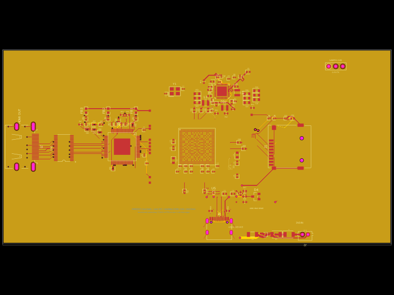
shibosoftwaredev/f1c100s-linux-nema8-stepper-controller
Restores component part numbers and CAD models, removes test-point 3D bodies, and validates that solder paste exists only on top-side SMT pads without altering copper or DRC.
- Version
- 0.3.5
- License
- unset
- Stars
- 0
modules/f1c100s/src/saved-paths.tsx
import type { FanoutTracePath } from "@tscircuit/props";
import type {
	GenericLocalAutorouter,
	SimpleRouteJson,
	Subcircuit,
} from "tscircuit";
import type { LayoutProfile } from "./profiles";
import native from "./generated/native.trace-paths.json";
import lcdTopStorageRight from "./generated/lcd_top_storage_right.trace-paths.json";
import lcdRightStorageBottom from "./generated/lcd_right_storage_bottom.trace-paths.json";
import lcdTopStorageBottom from "./generated/lcd_top_storage_bottom.trace-paths.json";
import lcdRightStorageLeft from "./generated/lcd_right_storage_left.trace-paths.json";
const profiles = {
	native,
	lcd_top_storage_right: lcdTopStorageRight,
	lcd_right_storage_bottom: lcdRightStorageBottom,
	lcd_top_storage_bottom: lcdTopStorageBottom,
	lcd_right_storage_left: lcdRightStorageLeft,
};

const rootsWithPlatedLayerAccess = new WeakSet<object>();

/** The source board used 0.35 mm via lands in three especially dense fanout
 * junctions.  Expanding every land to the requested 0.45 mm requires spreading
 * those junctions so JLCPCB's 0.10 mm copper gap remains intact. */
function preparePaths(paths: FanoutTracePath[]): FanoutTracePath[] {
	const prepared = structuredClone(paths) as FanoutTracePath[];
	const moves = [
		{ from: [3.4, -9.25], to: [3.525, -9.15] },
		{ from: [3.65, -9.05], to: [3.525, -9.15] },
		{ from: [9.6, 2.8], to: [9.75, 2.675] },
		{ from: [9.9, 2.55], to: [9.75, 2.675] },
		// Collapse this original shared ground stitch at a clear point.  The
		// 0.45 mm barrel then clears SDMMC0_D{0,1,3} and the SPI0 escape while
		// its adjacent top/inner2 segments retain more than 0.10 mm spacing.
		{ from: [9.2, 0.2], to: [9, 1.4] },
		{ from: [9.2, 2.4], to: [9, 1.4] },
		// Keep the top-layer branch east of C_OSCO after leaving the stitch.
		{ from: [9.2, 1.735], to: [10.2, 1.4] },
		{ from: [9.225, 1.71], to: [12.2, 1.4] },
		{ from: [9.225, 2.485], to: [10.2, 1.4] },
		{ from: [2.35, 9.4], to: [2.475, 9.3] },
		{ from: [2.6, 9.2], to: [2.475, 9.3] },
	] as const;
	for (const path of prepared)
		for (const [index, point] of (path.route as any[]).entries()) {
			// Component-pad and breakout endpoints are immutable.
			if (index === 0 || index === path.route.length - 1) continue;
			const move = moves.find(
				({ from }) =>
					Math.abs(point.x - from[0]) < 1e-5 &&
					Math.abs(point.y - from[1]) < 1e-5,
			);
			if (move) [point.x, point.y] = move.to;
		}
	return prepared;
}

/** The pinned core drops pcb_port.layers when making router input. Restore
 * layer access from actual plated-hole obstacles immediately before routing,
 * for both saved fanouts and the carrier's configured local autorouter. */
function preservePlatedLayerAccess(instance: Subcircuit) {
	const root = instance.root!;
	if (rootsWithPlatedLayerAccess.has(root)) return;
	rootsWithPlatedLayerAccess.add(root);
	root.on(
		"autorouting:start",
		({ simpleRouteJson: input }: { simpleRouteJson: SimpleRouteJson }) => {
			if (!input) return;
			for (const connection of input.connections)
				for (const point of connection.pointsToConnect) {
					const hole = input.obstacles.find(
						(o) =>
							o.circuitJsonMetadata?.pcb_plated_hole_id &&
							Math.hypot(o.center.x - point.x, o.center.y - point.y) < 1e-5 &&
							(o.circuitJsonMetadata.pcb_port_id === point.pcb_port_id ||
								o.connectedTo.includes(
									connection.source_trace_id ?? connection.name,
								)),
					);
					if (hole) point.layers = [...hole.layers] as any;
				}
		},
	);
}

/** Every saved path on a net ends at the same junction. This final phase checks
 * that invariant; it never solves or invents copper. Parent routing is separate. */
export async function joinSavedPathExits(
	input: SimpleRouteJson,
): Promise<GenericLocalAutorouter> {
	for (const connection of input.connections) {
		const points = connection.pointsToConnect,
			first = points[0];
		// Core's SRJ currently defaults a physical port to its first layer.
		// A real plated barrel joins coincident exits on different layers.
		const barrel =
			first &&
			input.obstacles.find(
				(o) =>
					o.circuitJsonMetadata?.pcb_plated_hole_id &&
					Math.hypot(o.center.x - first.x, o.center.y - first.y) < 1e-4 &&
					o.connectedTo.some(
						(id) =>
							id === connection.name ||
							id === connection.source_trace_id ||
							points.some((p) => p.pcb_port_id === id),
					) &&
					points.every((p) =>
						(p.layers ?? [p.layer]).some((l) => o.layers.includes(l)),
					),
			);
		if (
			first &&
			points.some(
				(p) =>
					Math.hypot(p.x - first.x, p.y - first.y) > 1e-4 ||
					(!barrel &&
						!(p.layers ?? [p.layer]).some((l) =>
							(first.layers ?? [first.layer]).includes(l),
						)),
			)
		)
			throw new Error(`Saved F1C100S paths do not meet for ${connection.name}`);
	}
	const listeners: Record<string, ((event: any) => void)[]> = {
		complete: [],
		error: [],
		progress: [],
	};
	return {
		input,
		isRouting: false,
		on(event, listener) {
			listeners[event]!.push(listener);
		},
		start() {
			queueMicrotask(() =>
				listeners.complete!.forEach((f) => f({ type: "complete", traces: [] })),
			);
		},
		stop() {},
		solveSync() {
			return [];
		},
	};
}

/** Use the native saved-fanout API for copper, retaining the imported footprint
 * and schematic symbols. Electrical traces remain outside the fanout. */
export function attachSavedPaths(
	instance: Subcircuit,
	profile: LayoutProfile,
	paths?: FanoutTracePath[],
) {
	preservePlatedLayerAccess(instance);
	(instance as any)._isInflatedFromCircuitJson = false;
	const check = instance.doInitialPcbDesignRuleChecks.bind(instance);
	instance.doInitialPcbDesignRuleChecks = () => {
		deduplicateSharedVias(instance);
		check();
	};
	const module = instance.selectOne(".MODULE") as any;
	const components = [...module.children];
	module.add(
		<fanout
			name="COPPER"
			pcbX={0}
			pcbY={0}
			schLayout={{ layoutMode: "relative" }}
			pcbTracePaths={preparePaths(paths ?? profiles[profile] as FanoutTracePath[])}
		/>,
	);
	const fanout = module.selectOne(".COPPER");
	fanout._doInitialSchematicLayoutSections = () => {};
	for (const component of components) {
		module.children = module.children.filter((c: any) => c !== component);
		fanout.add(component);
	}
	for (const trace of instance.selectAll("trace") as any[]) {
		for (const props of [trace.props, trace._parsedProps]) {
			delete props.pcbPath;
			delete props.pcbStraightLine;
			props.maxLength = /^N_HOSC[IO]$/.test(props.name ?? "") ? 10 : 5000;
			if (/^N_HOSC[IO]$/.test(props.name ?? "")) props.maxViaCount = 0;
			props.path = props.path?.map((p: string) =>
				p.replace(".MODULE > ", ".MODULE .COPPER > "),
			);
		}
	}
}

/** Core currently emits a via for every path that shares it. Keep one physical
 * drill per same-net location before either native or independent DRC runs. */
function deduplicateSharedVias(instance: Subcircuit) {
	const db = instance.root!.db;
	const seen = new Map<string, string>();
	for (const via of db.pcb_via.list()) {
		if (via.subcircuit_id !== instance.subcircuit_id) continue;
		const key = [
			via.x.toFixed(6),
			via.y.toFixed(6),
			via.hole_diameter,
			via.outer_diameter,
			[...via.layers].sort().join(","),
		].join(":");
		const traceId = db.pcb_trace.get(via.pcb_trace_id!)?.source_trace_id;
		// Separate pin-to-cap traces can belong to one electrical supply net.
		const net =
			(traceId &&
				db.source_trace.get(traceId)?.subcircuit_connectivity_map_key) ??
			traceId ??
			"";
		if (seen.has(key)) {
			if (seen.get(key) !== net)
				throw new Error("Different nets share an F1C100S via");
			db.pcb_via.delete(via.pcb_via_id);
		} else seen.set(key, net);
	}
}
Related Packages
 More from this authorShiboSoftwareDev/am625sip-linux-boardThis code defines the physical footprint and pin layout for an AM625 System-in-Package (SIP) component, detailing pad positions, pin labels, and package outline for hardware integration.
 Similar packageaura/diy-power-delivery-triggerThis hardware design implements a USB Type-C port with supporting power management and signal conditioning components, including a USB-C connector, a FUSB302 USB-C port controller, ESD protection diodes, a buck converter for 3.3V power regulation, an STM32 microcontroller for control and processing, an RGB LED indicator, push button, terminal block connections, and associated filtering and support components.
 Discover something newtscircuit/standard-jst-programmer26 × 42 mm USB-C RP2040 programmer with JST and TC2030 IDC SWD, NRST, selectable sensed 5 V / 3.3 V power, RGB status, and importable JST SH/Tag-Connect targets. Top-side assembly.