shibosoftwaredev/f1c100s-linux-nema8-stepper-controller
Restores component part numbers and CAD models, removes test-point 3D bodies, and validates that solder paste exists only on top-side SMT pads without altering copper or DRC.
- Version
- 0.3.5
- License
- unset
- Stars
- 0
index.circuit.tsx
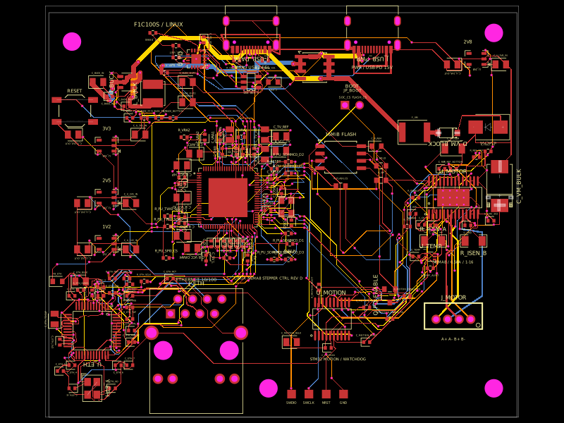
PCB
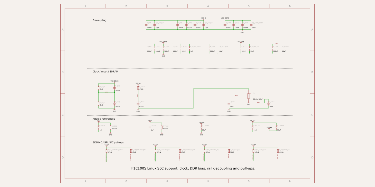
Schematic
import { footprints } from "./footprints"
import { MotorStage } from "./motor-stage"
import { PdPower, UsbPowerPort } from "./pd-power"
import { EthernetSection } from "./ethernet"
import { MotionController } from "./motion-controller"
import { fixedBoardRouter } from "./fixed-board-router"
import { routingBoundaryRef, routingKeepoutRef } from "./routing-boundary"
import {
  F1C100SModule,
  F1C100SLcdSchematicBox,
  F1C100SStorageSchematicBox,
  F1C100SGpioSchematicBox,
  F1C100SAudioSchematicBox,
  F1C100SVideoTouchSchematicBox,
  F1C100SSystemSchematicBox,
  F1C100SPowerSchematicBox,
} from "./modules/f1c100s/src"
import { ElectricalCorrections } from "./electrical-corrections"

// 4-layer carrier; the imported module includes stored copper on all four layers.
const connect = (part: string, nets: string[]) => nets.map((net, i) =>
  net ? <trace key={`${part}-${i}`} from={`.${part} > .pin${i + 1}`} to={`net.${net}`} /> : null)
const cap = (name: string, value: string, net: string, x: number, y: number, rotation = 0, target?: string, schX = x, schY = y, schSheetName?: string) => <>
  <capacitor name={name} capacitance={value} footprint={value === "4.7uF" ? "0805" : "0603"} maxVoltageRating={value === "4.7uF" ? 16 : undefined} manufacturerPartNumber={value === "4.7uF" ? "GRM21BR71C475KE51L" : undefined} pcbX={x} pcbY={y} pcbRotation={rotation} schX={schX} schY={schY} schSheetName={schSheetName} />
  <trace from={`.${name} > .pin1`} to={target ?? `net.${net}`} maxLength={target ? 15 : undefined} />
  <trace from={`.${name} > .pin2`} to="net.BOARD_GND" maxLength={1000} />
</>
const resistor = (name: string, value: string, a: string, b: string, x: number, y: number, schX = x, schY = y, schSheetName?: string) => <>
  <resistor name={name} resistance={value} footprint="0603" pcbX={x} pcbY={y} schX={schX} schY={schY} schSheetName={schSheetName} />
  {connect(name, [a, b])}
</>
const primaryLdo = (name: string, input: string, output: string, x: number, y: number, schX: number, schY: number) => <>
  <chip name={name} manufacturerPartNumber="AP2112K-3.3TRG1"
    supplierPartNumbers={{jlcpcb:["C51118"]}}
    footprint="dfn6_missing(5)_p0.95mm_w3.5mm_pw0.5mm_pl0.9mm_pin1location(rightside,bottom)"
    pinLabels={{pin1:"IN",pin2:"GND",pin3:"EN",pin4:"NC",pin5:"OUT",pin6:"NC6",pin7:"NC7",pin8:"NC8"}}
    pinAttributes={{pin2:{requiresGround:true},pin4:{doNotConnect:true},pin6:{doNotConnect:true},pin7:{doNotConnect:true},pin8:{doNotConnect:true}}}
    pcbX={x} pcbY={y} schX={schX} schY={schY} schSheetName="power_rails" />
  {/* Keep five connection records so the frozen carrier routing remains stable. */}
  <trace from={`.${name} > .pin5`} to={`net.${output}`} />
  <trace from={`.${name} > .pin3`} to={`net.${input}`} />
  <trace from={`.${name} > .pin2`} to="net.BOARD_GND" />
  <trace from={`.${name} > .pin2`} to="net.BOARD_GND" />
  <trace from={`.${name} > .pin1`} to={`net.${input}`} />
  {cap(`C_${name}_IN`, "4.7uF", input, x+5.8, y+1.905, 0, `.${name} > .pin1`, schX+5, schY+1.5, "power_rails")}
  {cap(`C_${name}_OUT`, "4.7uF", output, x-5.8, y+1.905, 180, `.${name} > .pin5`, schX-5, schY+1.5, "power_rails")}
</>

// AP2112K SOT-25: input 1, ground 2, enable 3, NC 4, output 5.
const ldoK = (name: string, voltage: string, output: string, x: number, y: number, schX: number, schY: number, mpn = `AP2112K-${voltage}TRG1`) => <>
  <chip name={name} manufacturerPartNumber={mpn}
    footprint="dfn6_missing(5)_p0.95mm_w3.5mm_pw0.5mm_pl0.9mm_pin1location(rightside,bottom)"
    pinLabels={{pin1:"IN",pin2:"GND",pin3:"EN",pin4:"NC",pin5:"OUT"}}
    pinAttributes={{pin2:{requiresGround:true},pin4:{doNotConnect:true}}}
    pcbX={x} pcbY={y} schX={schX} schY={schY} schSheetName="power_rails" />
  {connect(name, ["V3V3","","V3V3","",output])}
  {cap(`C_${name}_IN`, "4.7uF", "V3V3", x+4.2, y-0.95, 0, `.${name} > .pin1`, schX+4, schY-1.5, "power_rails")}
  {cap(`C_${name}_OUT`, "4.7uF", output, x-4.2, y-0.95, 180, `.${name} > .pin5`, schX-4, schY-1.5, "power_rails")}
  <trace name={`${name}_LOCAL_GND`} from={`.${name} > .pin2`} to={`.C_${name}_OUT > .pin2`}
    pcbPath={[`.${name} > .pin2`,{x:-2.5,y:0},{x:-2.5,y:-2},{x:-5.1125,y:-2},`.C_${name}_OUT > .pin2`]} />
</>

export default () => <board outline={[{x:-31,y:-38},{x:50,y:-38},{x:50,y:32},{x:-31,y:32}]} layers={4}
  minTraceWidth={0.12} minViaPadDiameter={0.45} minViaHoleDiameter={0.3}
  pcbStyle={{viaPadDiameter:0.45, viaHoleDiameter:0.3}}
  isViaInPadAllowed
  autorouter="auto-local" autorouterEffortLevel="2x"
  {...{ref:routingBoundaryRef}} schLayout={{layoutMode:"relative"}} schTraceAutoLabelEnabled schMaxTraceDistance={3}>
  {/* Keep each functional block readable on its own drawing. Components use
      schSheetName below; these declarations provide titles and sheet-local
      notes without changing PCB order or placement. */}
  <schematicsheet name="soc_support" displayName="1 — F1C100S support" sheetIndex={1} sheetSize="A4">
    <schematictext text="F1C100S Linux SoC support: clock, DDR bias, rail decoupling and pull-ups." schX={0} schY={-12.2} fontSize={0.42} />
  </schematicsheet>
  <schematicsheet name="linux_io" displayName="2 — Linux interfaces" sheetIndex={2} sheetSize="ANSI_B">
    <F1C100SSystemSchematicBox moduleName="SOC" schX={-14} schY={5} />
    <F1C100SStorageSchematicBox moduleName="SOC" schX={0} schY={5} />
    <F1C100SGpioSchematicBox moduleName="SOC" schX={14} schY={5} />
    <schematictext text="Boot flash, reset and USB2/FEL data interface. Ethernet and motion links continue by net label." schX={0} schY={-12.2} fontSize={0.42} />
  </schematicsheet>
  <schematicsheet name="soc_unused" displayName="3 — Unused SoC interfaces" sheetIndex={3} sheetSize="A4">
    <F1C100SLcdSchematicBox moduleName="SOC" schX={-8} schY={4.5} />
    <F1C100SAudioSchematicBox moduleName="SOC" schX={6} schY={4.5} />
    <F1C100SVideoTouchSchematicBox moduleName="SOC" schX={0} schY={-4.5} />
    <schematictext text="Unused F1C100S LCD, audio, video and touch pins are documented here; they are not external expansion headers." schX={0} schY={-12.2} fontSize={0.42} />
  </schematicsheet>
  <schematicsheet name="pd_power" displayName="4 — USB-C PD and 5 V" sheetIndex={4} sheetSize="ANSI_B">
    <schematictext text="Dedicated USB-C PD power input requests 15 V / 3 A. The separate USB-C data port is USB2/FEL only." schX={0} schY={-12.2} fontSize={0.42} />
  </schematicsheet>
  <schematicsheet name="power_rails" displayName="5 — SoC power rails" sheetIndex={5} sheetSize="A4">
    <F1C100SPowerSchematicBox moduleName="SOC" schX={-8} schY={4.5} />
    <schematictext text="Dedicated 3.3 V, 2.8 V, 2.5 V and 1.2 V rails. Regulator ratings are device limits, not a board load budget." schX={0} schY={-12.2} fontSize={0.42} />
  </schematicsheet>
  <schematicsheet name="ethernet" displayName="6 — 10/100 Ethernet" sheetIndex={6} sheetSize="ANSI_B">
    <schematictext text="W5500 Ethernet over SPI with integrated-magnetics RJ45 and reference termination network." schX={0} schY={-12.2} fontSize={0.42} />
  </schematicsheet>
  <schematicsheet name="motion" displayName="7 — Real-time stepper control" sheetIndex={7} sheetSize="ANSI_B">
    <schematictext text="STM32 watchdog motion controller and DRV8825 stage for StepperOnline 8HS15-0604S NEMA 8, 15 V, 0.58 A peak/phase, fixed 1/16 microstep." schX={0} schY={-13.2} fontSize={0.42} />
  </schematicsheet>
  {/* Routing-only reservations protect the verified, stored Linux-module fanout. */}
  <keepout shape="rect" width={25.6} height={25.6} pcbX={0} pcbY={0}
    layers={["top","inner1","inner2","bottom"]} excludeRefs={[".SOC *"]} {...{ref:routingKeepoutRef}} />
  <keepout shape="rect" width={0.8} height={1.1} pcbX={13.3} pcbY={2.65}
    layers={["top","inner1","inner2","bottom"]} excludeRefs={[".SOC *"]} {...{ref:routingKeepoutRef}} />
  {/* Preserve the imported carrier's large-hole clearance during aggregate-net routing. */}
  <keepout shape="rect" width={4} height={4} pcbX={-11.215} pcbY={-26.445}
    layers={["top","inner1","inner2","bottom"]} excludeRefs={[".J_ETH"]} {...{ref:routingKeepoutRef}} />
  <keepout shape="rect" width={4} height={4} pcbX={0.215} pcbY={-26.445}
    layers={["top","inner1","inner2","bottom"]} excludeRefs={[".J_ETH"]} {...{ref:routingKeepoutRef}} />
  <keepout shape="rect" width={5} height={0.8} pcbX={-25} pcbY={-19.73}
    layers={["top","inner1","inner2","bottom"]} excludeRefs={[".U_ETH"]} {...{ref:routingKeepoutRef}} />
  <keepout shape="rect" width={0.8} height={0.8} pcbX={-25.37} pcbY={-15.37}
    layers={["top","inner1","inner2","bottom"]} excludeRefs={[".C_ETH_BULK", ".R_ETH_EXRES"]} {...{ref:routingKeepoutRef}} />
  <keepout shape="rect" width={0.8} height={0.8} pcbX={-26.77} pcbY={-20.36}
    layers={["top","inner1","inner2","bottom"]} excludeRefs={[".U_ETH"]} {...{ref:routingKeepoutRef}} />
  <keepout shape="rect" width={0.8} height={0.8} pcbX={-25.16} pcbY={-17.78}
    layers={["top","inner1","inner2","bottom"]} excludeRefs={[".U_ETH", ".R_ETH_EXRES"]} {...{ref:routingKeepoutRef}} />
  <net name="BOARD_GND" isGroundNet nominalTraceWidth={0.3} />
  <net name="VBUS_PD" nominalTraceWidth={0.8} />
  <net name="V5_LOGIC" nominalTraceWidth={0.5} />
  <net name="PD_VDD" nominalTraceWidth={0.15} />
  <net name="V3V3" nominalTraceWidth={0.12} />
  <net name="ETH_3V3" nominalTraceWidth={0.25} />
  <net name="V2V8" nominalTraceWidth={0.12} />
  <net name="V2V5" nominalTraceWidth={0.12} />
  <net name="V1V2" nominalTraceWidth={0.12} />
  <F1C100SModule name="SOC" layoutProfile="native" schematicLayout="custom"
    pcbX={0} pcbY={0} schX={0} schY={-2} schSheetName="soc_support"
    connections={{
      GND:"net.BOARD_GND", VDD_CORE:"net.V1V2", VCC_DRAM:"net.V2V5",
      VCC_IO:"net.V3V3", VCC_USB:"net.V3V3", AVCC:"net.V2V8",
      VCC_HP:"net.V3V3", VCC_TV:"net.V3V3",
      SPI0_CLK:"net.FLASH_CLK", SPI0_CS:"net.SOC_FLASH_CS",
      SPI0_MOSI:"net.FLASH_MOSI", SPI0_MISO:"net.FLASH_MISO",
      PE7:"net.ETH_CS", PE8:"net.ETH_MOSI", PE9:"net.ETH_SCLK_SOC", PE10:"net.ETH_MISO",
      UART0_TX:"net.MOTION_RX", UART0_RX:"net.MOTION_TX",
      USB_DM:"net.USB_N", USB_DP:"net.USB_P", RESET:"net.RESET_N",
      PE2:"net.MOTION_BOOT", PE3:"net.MOTION_NRST",
      PE5:"net.ETH_RST", PE6:"net.ETH_INT",
    }} />

  <PdPower />
  <EthernetSection />
  <MotionController />
  <resistor name="R_ETH_SCLK" resistance="0" footprint="0402"
    supplierPartNumbers={{jlcpcb:["C2906877"]}} pcbX={-14.5} pcbY={-14.5}
    schX={8} schY={10} schSheetName="ethernet" />
  <trace name="ETH_SCLK_SOC_LINK" from=".R_ETH_SCLK > .pin2" to="net.ETH_SCLK_SOC" thickness={0.15} />
  <trace name="ETH_SCLK_DIRECT" from=".R_ETH_SCLK > .pin1" to=".U_ETH > .SCLK" thickness={0.15}
    pcbPath={[".R_ETH_SCLK > .pin1",
      {x:-0.51,y:-1}, {x:-0.51,y:-1,via:true,fromLayer:"top",toLayer:"inner2"}, {x:-0.51,y:-1},
      {x:-10.4,y:-1}, {x:-10.4,y:-4.9}, {x:-10.5,y:-4.9},
      {x:-10.5,y:-5.9}, {x:-10.4,y:-5.9}, {x:-10.4,y:-13.7}, {x:-7.75,y:-13.7},
      {x:-7.75,y:-13.7,via:true,fromLayer:"inner2",toLayer:"top"}, {x:-7.75,y:-13.7},
      ".U_ETH > .SCLK"]} />
  {/* The HUSB238A open-drain contract-valid signal crosses the board on the
      bottom layer. Fixed vias keep the QFN escape away from adjacent VBUS. */}
  <trace name="PD_GOOD_REMOTE" from=".U_PD > .GATE" to=".Q_PD_ENABLE > .G" thickness={0.15}
    pcbPath={[".U_PD > .GATE",
      {x:-2.6,y:-0.25}, {x:-2.6,y:-0.25,via:true,fromLayer:"top",toLayer:"bottom"},
      {x:-2.6,y:-0.25},
      {x:-5.2,y:-4}, {x:-5.2,y:-8.3},
      {x:-5.6,y:-8.3}, {x:-5.6,y:-9.7}, {x:-5.2,y:-9.7},
      {x:-5.2,y:-12.5}, {x:-24.35,y:-31.7},
      {x:-34.18,y:-31.72}, {x:-34.18,y:-31.72,via:true,fromLayer:"bottom",toLayer:"top"},
      {x:-34.18,y:-31.72},
      {x:-37.15,y:-31.75}, ".Q_PD_ENABLE > .G"]} />

  {/* AP2112K SOT-25: output 1, ground 2, enable 3, input 5. */}
  {primaryLdo("U_3V3", "V5_LOGIC", "V3V3", -21, 9, 5, 6)}
  {ldoK("U_2V5", "2.5", "V2V5", -21, 0, 5, 1)}
  {ldoK("U_1V2", "1.2", "V1V2", -21, -8, 5, -4)}
  {/* Codec AVCC requires 2.5–3.1 V; dedicated 2.8 V supply. */}
  {ldoK("U_2V8", "2.8", "V2V8", 43, 24, -6, -4, "TPAP2127K-2.8TRG1")}

  {/* 16 MiB SPI NOR for SPL / U-Boot / compact Linux + rootfs. */}
  <chip name="U_FLASH" manufacturerPartNumber="W25Q128JVSIQ"
    footprint={footprints.flash}
    pinLabels={{pin1:"CS_N",pin2:"DO",pin3:"WP_N",pin4:"BOARD_GND",pin5:"DI",pin6:"CLK",pin7:"HOLD_N",pin8:"VCC"}}
    pcbX={19.5} pcbY={7} schX={5} schY={-2} schSheetName="linux_io" />
  {connect("U_FLASH", ["FLASH_CS","FLASH_MISO","","BOARD_GND","FLASH_MOSI","FLASH_CLK","FLASH_HOLD","V3V3"])}
  {cap("C_FLASH", "100nF", "V3V3", 25.7, 8.905, 0, ".U_FLASH > .pin8", 10, -2, "linux_io")}
  {resistor("R_WP", "10k", "FLASH_WP", "V3V3", 26.5, 3, 10, -5, "linux_io")}
  <trace name="FLASH_WP_DIRECT" from=".U_FLASH > .WP_N" to=".R_WP > .pin1" thickness={0.15}
    pcbPath={[".U_FLASH > .WP_N",
      {x:-5,y:-0.635}, {x:-5,y:-0.635,via:true,fromLayer:"top",toLayer:"inner1"}, {x:-5,y:-0.635},
      {x:-5,y:-5.5}, {x:6.175,y:-5.5},
      {x:6.175,y:-5.5,via:true,fromLayer:"inner1",toLayer:"top"}, {x:6.175,y:-5.5},
      ".R_WP > .pin1"]} />
  {resistor("R_HOLD", "10k", "FLASH_HOLD", "V3V3", 26.5, 5.5, 10, -3.5, "linux_io")}
  {resistor("R_FLASH_CS", "10k", "FLASH_CS", "V3V3", 19.5, 2, 1, -5, "linux_io")}
  <chip name="JP_BOOT" footprint="pinrow2_p2.54" pinLabels={{pin1:"SOC_CS",pin2:"FLASH_CS"}}
    pcbX={21.5} pcbY={16} schX={5} schY={-8} schSheetName="linux_io" />
  {connect("JP_BOOT", ["SOC_FLASH_CS","FLASH_CS"])}

  <chip name="SW_RESET" footprint={footprints.reset}
    manufacturerPartNumber="TL3342F160QG" pinLabels={{pin1:"RESET",pin2:"BOARD_GND"}}
    pcbX={-26.5} pcbY={15} schX={-13} schY={-5} schSheetName="linux_io" />
  {connect("SW_RESET", ["RESET_N","BOARD_GND"])}
  {/* USBLC6-2SC6: shunt ESD protection; duplicate IO pads are internally common. */}
  <chip name="U_USB_ESD" manufacturerPartNumber="USBLC6-2SC6" footprint="sot23_6"
    pinLabels={{pin1:"DM1",pin2:"BOARD_GND",pin3:"DP1",pin4:"DP2",pin5:"VBUS",pin6:"DM2"}}
    pcbX={4} pcbY={20} pcbRotation={180} schX={-9} schY={-2} schSheetName="linux_io" />
  {connect("U_USB_ESD", ["USB_N","BOARD_GND","USB_P","","V3V3",""])}
  <trace name="ESD_DM_BRIDGE" from=".U_USB_ESD > .pin1" to=".U_USB_ESD > .pin6" thickness={0.15}
    pcbPath={[".U_USB_ESD > .pin1", {x:-1.3,y:1.6}, {x:1.3,y:1.6}, ".U_USB_ESD > .pin6"]} />
  <trace name="ESD_DP_BRIDGE" from=".U_USB_ESD > .pin3" to=".U_USB_ESD > .pin4" thickness={0.15}
    pcbPath={[".U_USB_ESD > .pin3", {x:-1.3,y:-1.6}, {x:1.3,y:-1.6}, ".U_USB_ESD > .pin4"]} />
  {cap("C_ESD", "100nF", "V3V3", 7.8, 20, 180, ".U_USB_ESD > .pin5", -4, -2, "linux_io")}

  <MotorStage />
  {/* Render the new connector last so all established component/port IDs stay
      stable for the deterministic fabrication routing. */}
  <UsbPowerPort />
  {/* Added after the frozen carrier to preserve all established component and
      trace identifiers used by the deterministic board router. */}
  <ElectricalCorrections />

  <hole name="H_NW" diameter={3.2} pcbX={-27} pcbY={27} />
  <hole name="H_NE" diameter={3.2} pcbX={46} pcbY={28.5} />
  <hole name="H_SW" diameter={3.2} pcbX={7} pcbY={-33} />
  <hole name="H_SE" diameter={3.2} pcbX={46} pcbY={-33} />
  <silkscreentext text="RESET" pcbX={-26.5} pcbY={18.5} fontSize={0.8} />
  <silkscreentext text="3V3" pcbX={-21} pcbY={12} fontSize={0.8} />
  <silkscreentext text="2V5" pcbX={-21} pcbY={3} fontSize={0.8} />
  <silkscreentext text="1V2" pcbX={-21} pcbY={-5} fontSize={0.8} />
  <silkscreentext text="2V8" pcbX={41.5} pcbY={27} fontSize={0.8} />
  <silkscreentext text="LINUX NEMA8 STEPPER CTRL REV D" pcbX={7} pcbY={-14} fontSize={0.65} />
  <silkscreentext text="16MiB FLASH" pcbX={19.5} pcbY={11} fontSize={0.8} />
  <silkscreentext text="F1C100S / LINUX" pcbX={-12} pcbY={30} fontSize={1.0} />
  <silkscreentext text="BOOT" pcbX={21.5} pcbY={19.3} fontSize={0.8} />
  {/* Ground is routed explicitly on all four layers. Copper-pour generation is
      intentionally omitted because the current core release crashes in its
      floating-island cleanup for this dense, via-in-pad four-layer layout. */}
  <autoroutingphase autorouter="auto-local" algorithmFn={fixedBoardRouter}
    minTraceToPadEdgeClearance={0.1} minPadEdgeToPadEdgeClearance={0.1} minViaEdgeToPadEdgeClearance={0.1} />
</board>
Related Packages
 More from this authorShiboSoftwareDev/am625sip-linux-boardThis code defines the physical footprint and pin layout for an AM625 System-in-Package (SIP) component, detailing pad positions, pin labels, and package outline for hardware integration.
 Similar packageaura/diy-power-delivery-triggerThis hardware design implements a USB Type-C port with supporting power management and signal conditioning components, including a USB-C connector, a FUSB302 USB-C port controller, ESD protection diodes, a buck converter for 3.3V power regulation, an STM32 microcontroller for control and processing, an RGB LED indicator, push button, terminal block connections, and associated filtering and support components.
 Discover something newtscircuit/standard-jst-programmer26 × 42 mm USB-C RP2040 programmer with JST and TC2030 IDC SWD, NRST, selectable sensed 5 V / 3.3 V power, RGB status, and importable JST SH/Tag-Connect targets. Top-side assembly.