shibosoftwaredev/f1c100s-linux-nema8-stepper-controller
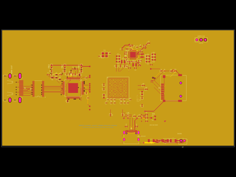
Restores component part numbers and CAD models, removes test-point 3D bodies, and validates that solder paste exists only on top-side SMT pads without altering copper or DRC.
- Version
- 0.3.5
- License
- unset
- Stars
- 0
imports/STM32G030F6P6.tsx
import type { ChipProps } from "@tscircuit/props"

const pinLabels = {
  pin1: ["PB7_PB8"],
  pin2: ["PB9_PC14_OSC32_IN"],
  pin3: ["PC15_OSC32_OUT"],
  pin4: ["VDD_VDDA"],
  pin5: ["VSS_VSSA"],
  pin6: ["NRST"],
  pin7: ["PA0"],
  pin8: ["PA1"],
  pin9: ["PA2"],
  pin10: ["PA3"],
  pin11: ["PA4"],
  pin12: ["PA5"],
  pin13: ["PA6"],
  pin14: ["PA7"],
  pin15: ["PB0_PB1_PB2_PA8"],
  pin16: ["PA11_PA9"],
  pin17: ["PA12_PA10"],
  pin18: ["PA13"],
  pin19: ["PA15_PA14_BOOT0"],
  pin20: ["PB3_PB4_PB5_PB6"]
} as const

const pinAttributes = {
  pin4: {requiresPower: true},
  pin5: {requiresGround: true},
} as const

export const STM32G030F6P6 = (props: ChipProps<typeof pinLabels>) => {
  return (
    <chip
      pinLabels={pinLabels}
      pinAttributes={pinAttributes}
      supplierPartNumbers={{
  "jlcpcb": [
    "C724040"
  ]
}}
      manufacturerPartNumber="STM32G030F6P6"
      footprint={<footprint>
        <smtpad portHints={["pin1"]} pcbX="-2.925064mm" pcbY="-2.870962mm" width="0.3640074mm" height="1.7420082mm" radius="0.1820037mm" shape="pill" />
<smtpad portHints={["pin2"]} pcbX="-2.275078mm" pcbY="-2.870962mm" width="0.3640074mm" height="1.7420082mm" radius="0.1820037mm" shape="pill" />
<smtpad portHints={["pin3"]} pcbX="-1.625092mm" pcbY="-2.870962mm" width="0.3640074mm" height="1.7420082mm" radius="0.1820037mm" shape="pill" />
<smtpad portHints={["pin4"]} pcbX="-0.975106mm" pcbY="-2.870962mm" width="0.3640074mm" height="1.7420082mm" radius="0.1820037mm" shape="pill" />
<smtpad portHints={["pin5"]} pcbX="-0.324866mm" pcbY="-2.870962mm" width="0.3640074mm" height="1.7420082mm" radius="0.1820037mm" shape="pill" />
<smtpad portHints={["pin6"]} pcbX="0.32512mm" pcbY="-2.870962mm" width="0.3640074mm" height="1.7420082mm" radius="0.1820037mm" shape="pill" />
<smtpad portHints={["pin7"]} pcbX="0.975106mm" pcbY="-2.870962mm" width="0.3640074mm" height="1.7420082mm" radius="0.1820037mm" shape="pill" />
<smtpad portHints={["pin8"]} pcbX="1.625092mm" pcbY="-2.870962mm" width="0.3640074mm" height="1.7420082mm" radius="0.1820037mm" shape="pill" />
<smtpad portHints={["pin9"]} pcbX="2.275078mm" pcbY="-2.870962mm" width="0.3640074mm" height="1.7420082mm" radius="0.1820037mm" shape="pill" />
<smtpad portHints={["pin10"]} pcbX="2.925064mm" pcbY="-2.870962mm" width="0.3640074mm" height="1.7420082mm" radius="0.1820037mm" shape="pill" />
<smtpad portHints={["pin20"]} pcbX="-2.925064mm" pcbY="2.870962mm" width="0.3640074mm" height="1.7420082mm" radius="0.1820037mm" shape="pill" />
<smtpad portHints={["pin19"]} pcbX="-2.275078mm" pcbY="2.870962mm" width="0.3640074mm" height="1.7420082mm" radius="0.1820037mm" shape="pill" />
<smtpad portHints={["pin18"]} pcbX="-1.625092mm" pcbY="2.870962mm" width="0.3640074mm" height="1.7420082mm" radius="0.1820037mm" shape="pill" />
<smtpad portHints={["pin17"]} pcbX="-0.975106mm" pcbY="2.870962mm" width="0.3640074mm" height="1.7420082mm" radius="0.1820037mm" shape="pill" />
<smtpad portHints={["pin16"]} pcbX="-0.324866mm" pcbY="2.870962mm" width="0.3640074mm" height="1.7420082mm" radius="0.1820037mm" shape="pill" />
<smtpad portHints={["pin15"]} pcbX="0.32512mm" pcbY="2.870962mm" width="0.3640074mm" height="1.7420082mm" radius="0.1820037mm" shape="pill" />
<smtpad portHints={["pin14"]} pcbX="0.975106mm" pcbY="2.870962mm" width="0.3640074mm" height="1.7420082mm" radius="0.1820037mm" shape="pill" />
<smtpad portHints={["pin13"]} pcbX="1.625092mm" pcbY="2.870962mm" width="0.3640074mm" height="1.7420082mm" radius="0.1820037mm" shape="pill" />
<smtpad portHints={["pin12"]} pcbX="2.275078mm" pcbY="2.870962mm" width="0.3640074mm" height="1.7420082mm" radius="0.1820037mm" shape="pill" />
<smtpad portHints={["pin11"]} pcbX="2.925064mm" pcbY="2.870962mm" width="0.3640074mm" height="1.7420082mm" radius="0.1820037mm" shape="pill" />
<silkscreenpath route={[{"x":-3.326206200000115,"y":-1.7713960000000952},{"x":-3.326206200000115,"y":1.7713959999999815},{"x":3.3262061999998878,"y":1.7713959999999815},{"x":3.3262061999998878,"y":-1.7713960000000952},{"x":-3.326206200000115,"y":-1.7713960000000952}]} />
<silkscreencircle pcbX="-2.925064mm" pcbY="-1.019048mm" radius="0.150114mm" />
<silkscreencircle pcbX="-3.559302mm" pcbY="-2.870962mm" radius="0.150114mm" />
<silkscreentext text="{NAME}" pcbX="-0.1905mm" pcbY="4.556mm" anchorAlignment="center" fontSize="1mm" />
<courtyardoutline outline={[{"x":-3.958400000000097,"y":3.80600000000004},{"x":3.5773999999998978,"y":3.80600000000004},{"x":3.5773999999998978,"y":-4.009199999999964},{"x":-3.958400000000097,"y":-4.009199999999964},{"x":-3.958400000000097,"y":3.80600000000004}]} />
      </footprint>}
      cadModel={{
        objUrl: "https://modelcdn.tscircuit.com/easyeda_models/assets/C724040.obj?uuid=f8ba5b4174b9490d8c445fbe2ed40b80",
        stepUrl: "https://modelcdn.tscircuit.com/easyeda_models/assets/C724040.step?uuid=f8ba5b4174b9490d8c445fbe2ed40b80",
        pcbRotationOffset: 90,
        modelOriginPosition: { x: 0, y: 0.000012700000070253736, z: -0.019205 },
      }}
      {...props}
    />
  )
}
Related Packages
 More from this authorShiboSoftwareDev/am625sip-linux-boardThis code defines the physical footprint and pin layout for an AM625 System-in-Package (SIP) component, detailing pad positions, pin labels, and package outline for hardware integration.
 Similar packageaura/diy-power-delivery-triggerThis hardware design implements a USB Type-C port with supporting power management and signal conditioning components, including a USB-C connector, a FUSB302 USB-C port controller, ESD protection diodes, a buck converter for 3.3V power regulation, an STM32 microcontroller for control and processing, an RGB LED indicator, push button, terminal block connections, and associated filtering and support components.
 Discover something newtscircuit/standard-jst-programmer26 × 42 mm USB-C RP2040 programmer with JST and TC2030 IDC SWD, NRST, selectable sensed 5 V / 3.3 V power, RGB status, and importable JST SH/Tag-Connect targets. Top-side assembly.