seveibar/usbc-pd-charger
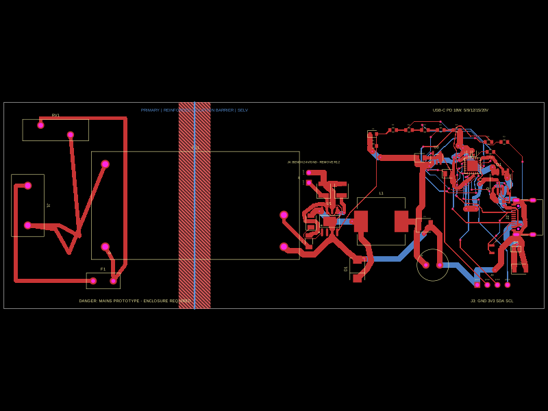
This code defines and assembles a hardware schematic of an 18W USB-C PD wall charger with mains input, protection, high-voltage isolation, a DC buck converter with switching regulator, filtering, and USB-C output with ESD protection.
- Version
- 1.0.2
- License
- unset
- Stars
- 0
index.circuit.tsx
PCB
Schematic

import { A_2010T1A250V } from "./imports/A_2010T1A250V"
import { A_7447709680 } from "./imports/A_7447709680"
import { WireTerminal } from "./imports/A_282838_2"
import { ESDA25P35_1U1M } from "./imports/ESDA25P35_1U1M"
import { IRM_20_24 } from "./imports/IRM_20_24"
import { MOV_14D471K } from "./imports/MOV_14D471K"
import { SI4925DDY_T1_GE3 } from "./imports/SI4925DDY_T1_GE3"
import { ST1S14PHR } from "./imports/ST1S14PHR"
import { STPS3L60U } from "./imports/STPS3L60U"
import { TPS7B6933QDBVRQ1 } from "./imports/TPS7B6933QDBVRQ1"
import { TYPE_C_16PIN_5A_143 } from "./imports/TYPE_C_16PIN_5A_143"

const stusb4710PinLabels = {
  pin1: ["NC1"],
  pin2: ["CC1"],
  pin3: ["NC3"],
  pin4: ["CC2"],
  pin5: ["NC5"],
  pin6: ["NC6"],
  pin7: ["SCL"],
  pin8: ["SDA"],
  pin9: ["NC9"],
  pin10: ["GND"],
  pin11: ["SEL_PDO3"],
  pin12: ["SEL_PDO2"],
  pin13: ["ADDR0"],
  pin14: ["SEL_PDO4"],
  pin15: ["SEL_PDO5"],
  pin16: ["NC16"],
  pin17: ["NC17"],
  pin18: ["VBUS_SENSE"],
  pin19: ["VBUS_DISCH"],
  pin20: ["VBUS_EN_SRC"],
  pin21: ["VREG_1V2"],
  pin22: ["NC22"],
  pin23: ["VREG_2V7"],
  pin24: ["VDD"],
  pin25: ["EP"],
} as const

const STUSB4710A = (props: {
  name: string
  pcbX: number
  pcbY: number
  schX: number
  schY: number
  schSheetName?: string
  schSectionName?: string
}) => (
  <chip
    {...props}
    pinLabels={stusb4710PinLabels}
    internallyConnectedPins={[["pin10", "pin25"]]}
    manufacturerPartNumber="STUSB4710AQTR"
    footprint={
      <footprint>
        <smtpad shape="rect" pcbX={-1.85} pcbY={1.25} width="0.65mm" height="0.25mm" portHints={["pin1"]} />
        <smtpad shape="rect" pcbX={-1.85} pcbY={0.75} width="0.65mm" height="0.25mm" portHints={["pin2"]} />
        <smtpad shape="rect" pcbX={-1.85} pcbY={0.25} width="0.65mm" height="0.25mm" portHints={["pin3"]} />
        <smtpad shape="rect" pcbX={-1.85} pcbY={-0.25} width="0.65mm" height="0.25mm" portHints={["pin4"]} />
        <smtpad shape="rect" pcbX={-1.85} pcbY={-0.75} width="0.65mm" height="0.25mm" portHints={["pin5"]} />
        <smtpad shape="rect" pcbX={-1.85} pcbY={-1.25} width="0.65mm" height="0.25mm" portHints={["pin6"]} />
        <smtpad shape="rect" pcbX={-1.25} pcbY={-1.85} width="0.25mm" height="0.65mm" portHints={["pin7"]} />
        <smtpad shape="rect" pcbX={-0.75} pcbY={-1.85} width="0.25mm" height="0.65mm" portHints={["pin8"]} />
        <smtpad shape="rect" pcbX={-0.25} pcbY={-1.85} width="0.25mm" height="0.65mm" portHints={["pin9"]} />
        <smtpad shape="rect" pcbX={0.25} pcbY={-1.85} width="0.25mm" height="0.65mm" portHints={["pin10"]} />
        <smtpad shape="rect" pcbX={0.75} pcbY={-1.85} width="0.25mm" height="0.65mm" portHints={["pin11"]} />
        <smtpad shape="rect" pcbX={1.25} pcbY={-1.85} width="0.25mm" height="0.65mm" portHints={["pin12"]} />
        <smtpad shape="rect" pcbX={1.85} pcbY={-1.25} width="0.65mm" height="0.25mm" portHints={["pin13"]} />
        <smtpad shape="rect" pcbX={1.85} pcbY={-0.75} width="0.65mm" height="0.25mm" portHints={["pin14"]} />
        <smtpad shape="rect" pcbX={1.85} pcbY={-0.25} width="0.65mm" height="0.25mm" portHints={["pin15"]} />
        <smtpad shape="rect" pcbX={1.85} pcbY={0.25} width="0.65mm" height="0.25mm" portHints={["pin16"]} />
        <smtpad shape="rect" pcbX={1.85} pcbY={0.75} width="0.65mm" height="0.25mm" portHints={["pin17"]} />
        <smtpad shape="rect" pcbX={1.85} pcbY={1.25} width="0.65mm" height="0.25mm" portHints={["pin18"]} />
        <smtpad shape="rect" pcbX={1.25} pcbY={1.85} width="0.25mm" height="0.65mm" portHints={["pin19"]} />
        <smtpad shape="rect" pcbX={0.75} pcbY={1.85} width="0.25mm" height="0.65mm" portHints={["pin20"]} />
        <smtpad shape="rect" pcbX={0.25} pcbY={1.85} width="0.25mm" height="0.65mm" portHints={["pin21"]} />
        <smtpad shape="rect" pcbX={-0.25} pcbY={1.85} width="0.25mm" height="0.65mm" portHints={["pin22"]} />
        <smtpad shape="rect" pcbX={-0.75} pcbY={1.85} width="0.25mm" height="0.65mm" portHints={["pin23"]} />
        <smtpad shape="rect" pcbX={-1.25} pcbY={1.85} width="0.25mm" height="0.65mm" portHints={["pin24"]} />
        <smtpad shape="rect" pcbX={0} pcbY={0} width="2.7mm" height="2.7mm" portHints={["pin25"]} />
        <silkscreenrect pcbX={0} pcbY={0} width="4mm" height="4mm" />
        <silkscreencircle pcbX={-2.1} pcbY={1.6} radius="0.2mm" />
      </footprint>
    }
  />
)

const RadialElectrolytic = (props: {
  name: string
  capacitance: string
  maxVoltageRating: string
  pcbX: number
  pcbY: number
  schX: number
  schY: number
  schSheetName?: string
  schSectionName?: string
}) => (
  <capacitor
    {...props}
    footprint={
      <footprint>
        <platedhole
          shape="circle"
          holeDiameter="0.9mm"
          outerDiameter="1.8mm"
          pcbX="-1.75mm"
          portHints={["pin1", "positive"]}
        />
        <platedhole
          shape="circle"
          holeDiameter="0.9mm"
          outerDiameter="1.8mm"
          pcbX="1.75mm"
          portHints={["pin2", "negative"]}
        />
        <silkscreencircle pcbX={0} pcbY={0} radius="4mm" />
        <silkscreentext text="+" pcbX="-2.7mm" pcbY="2.4mm" fontSize="1mm" />
      </footprint>
    }
  />
)

/**
 * 18 W USB-C PD source for 120 Vac nominal (85-305 Vac module rating).
 *
 * Architecture:
 *   protected AC input -> reinforced-isolation IRM-20-24 -> ST1S14 buck
 *   -> back-to-back PMOS load switch -> USB-C receptacle.
 *
 * The STUSB4710A must be NVM-programmed before use. See PD_PROGRAMMING.md.
 */
export default () => (
  <board
    name="US_PD_WALL_CHARGER_18W"
    width="136mm"
    height="52mm"
    autorouter="auto"
    pcbStyle={{ viaPadDiameter: "0.6mm", viaHoleDiameter: "0.3mm" }}
    minViaPadDiameter="0.6mm"
    minViaHoleDiameter="0.3mm"
  >
    <net name="PSU24" />
    <net name="VIN24" />
    <net name="GND" isGroundNet />
    <net name="SW" />
    <net name="BOOT" />
    <net name="VSRC" />
    <net name="FB" />
    <net name="FB_20" />
    <net name="FB_15" />
    <net name="FB_12" />
    <net name="FB_9" />
    <net name="V3V3" />
    <net name="VREG1V2" />
    <net name="VREG2V7" />
    <net name="ADDR0" />
    <net name="EN_SRC" />
    <net name="SCL" />
    <net name="SDA" />
    <net name="CC1" />
    <net name="CC2" />
    <net name="QCOMMON" />
    <net name="GATE" />
    <net name="VBUS" />

    <schematicsheet
      name="main"
      displayName="18 W USB-C PD Wall Charger"
      sheetIndex={0}
    >
      <schematicsection name="ac_input" displayName="1. AC Input & Protection" sectionTitleFontSize={0.22} />
      <schematicsection name="isolated_supply" displayName="2. Isolated 24 V Supply" sectionTitleFontSize={0.22} />
      <schematicsection name="buck_power" displayName="3. Programmable Buck Stage" sectionTitleFontSize={0.22} />
      <schematicsection name="feedback" displayName="4. Feedback & PDO Selection" sectionTitleFontSize={0.22} />
      <schematicsection name="pd_control" displayName="5. USB-PD Control & I2C" sectionTitleFontSize={0.22} />
      <schematicsection name="usb_output" displayName="6. Protected USB-C Output" sectionTitleFontSize={0.22} />
    </schematicsheet>

    {/* Primary/secondary isolation corridor. The keepout prevents the router
        from placing copper across the barrier beneath the approved module. */}
    <keepout
      shape="rect"
      pcbX={-20}
      pcbY={0}
      width="8mm"
      height="52mm"
      layers={["top", "bottom"]}
    />
    <pcbnoteline x1={-20} y1={-26} x2={-20} y2={26} strokeWidth="0.4mm" isDashed />
    <pcbnotetext text="PRIMARY | REINFORCED ISOLATION BARRIER | SELV" pcbX={-20} pcbY={24} fontSize="1mm" />

    {/* AC input and protection. The direct wire-clamp terminal is rotated so
        its side-entry wire openings face outward at the left board edge. */}
    <WireTerminal name="J1" pcbX={-62} pcbY={0} pcbRotation={270} schX={-13} schY={6} schSheetName="main" schSectionName="ac_input" />
    <A_2010T1A250V name="F1" pcbX={-43} pcbY={-19} schX={-10} schY={6} schSheetName="main" schSectionName="ac_input" />
    <MOV_14D471K name="RV1" pcbX={-55} pcbY={19} schX={-10} schY={3.5} schSheetName="main" schSectionName="ac_input" />
    <IRM_20_24 name="PS1" pcbX={-20} pcbY={0} schX={-4} schY={6} schSheetName="main" schSectionName="isolated_supply" />

    {/* Keep all mains copper on the top layer with explicit routes. This avoids
        autorouter vias or opposite-layer overlap between line and neutral. */}
    <trace
      from=".J1 > .pin1"
      to=".F1 > .pin1"
      schDisplayLabel="LINE"
      width="1mm"
      pcbPathRelativeTo=".F1 > .pin1"
      pcbPath={[{ x: -22, y: 0 }, { x: -22, y: 24 }, { x: -19, y: 24 }]}
    />
    <trace
      from=".F1 > .pin2"
      to=".PS1 > .pin1"
      schDisplayLabel="LINE_FUSED"
      width="1mm"
      pcbPath={[{ x: 2.5, y: 5 }]}
    />
    <trace
      from=".F1 > .pin2"
      to=".RV1 > .pin1"
      width="1mm"
      pcbPath={[{ x: 5.5, y: 4 }, { x: 5.5, y: 41 }, { x: -15.75, y: 41 }]}
    />
    <trace
      from=".J1 > .pin2"
      to=".PS1 > .pin4"
      schDisplayLabel="NEUTRAL"
      width="1mm"
      pcbPath={[{ x: 6, y: 7 }, { x: 12, y: 10.4 }]}
    />
    <trace
      from=".J1 > .pin2"
      to=".RV1 > .pin2"
      width="1mm"
      pcbPath={[{ x: 5, y: 8 }, { x: 7.75, y: 13 }]}
    />
    <trace from=".PS1 > .pin3" to="net.PSU24" width="1mm" />
    <trace from=".PS1 > .pin2" to="net.GND" width="1mm" />

    {/* Low-voltage bring-up isolation. Populate R12 for normal AC operation.
        For isolated 24 V bench testing, remove R12 and inject at J4. */}
    <resistor name="R12" resistance="0" footprint="1206" pcbX={8.8} pcbY={-9} pcbRotation={90} schX={0} schY={6} schSheetName="main" schSectionName="isolated_supply" />
    <pinheader name="J4" pinCount={2} pitch="2.54mm" footprint="pinrow2" pcbX={8.8} pcbY={7} pcbRotation={90} schX={0} schY={3.5} schSheetName="main" schSectionName="isolated_supply" />
    <trace from=".R12 > .pin1" to="net.PSU24" width="1mm" />
    <trace from=".R12 > .pin2" to="net.VIN24" width="1mm" />
    <trace from=".J4 > .pin1" to="net.VIN24" width="1mm" />
    <trace from=".J4 > .pin2" to="net.GND" width="1mm" />

    {/* 24 V to negotiated VBUS buck converter, adapted from STEVAL-ISC004V1. */}
    <capacitor name="C1" capacitance="10uF" maxVoltageRating="50V" footprint="1210" pcbX={12.5} pcbY={4} pcbRotation={90} schX={6.5} schY={7.5} schSheetName="main" schSectionName="buck_power" />
    <capacitor name="C2" capacitance="10uF" maxVoltageRating="50V" footprint="1210" pcbX={17} pcbY={4} pcbRotation={90} schX={8} schY={7.5} schSheetName="main" schSectionName="buck_power" />
    <ST1S14PHR name="U1" pcbX={14} pcbY={-4} schX={9.5} schY={5.5} schSheetName="main" schSectionName="buck_power" />
    <capacitor name="C3" capacitance="220nF" maxVoltageRating="100V" footprint="1206" pcbX={9.3} pcbY={-4} pcbRotation={90} schX={9.5} schY={8.8} schSheetName="main" schSectionName="buck_power" />
    <STPS3L60U name="D1" pcbX={21} pcbY={-16} pcbRotation={90} schX={11.5} schY={3.5} schSheetName="main" schSectionName="buck_power" />
    <A_7447709680 name="L1" pcbX={27} pcbY={-4} schX={12} schY={5.5} schSheetName="main" schSectionName="buck_power" />
    <RadialElectrolytic name="C5" capacitance="220uF" maxVoltageRating="35V" pcbX={40} pcbY={-15} schX={14} schY={3.5} schSheetName="main" schSectionName="buck_power" />
    <capacitor name="C6" capacitance="22uF" maxVoltageRating="25V" footprint="1210" pcbX={38} pcbY={-5} schX={14} schY={5.5} schSheetName="main" schSectionName="buck_power" />

    <trace from=".C1 > .pin1" to="net.VIN24" width="0.8mm" />
    <trace from=".C1 > .pin2" to="net.GND" width="0.8mm" />
    <trace from=".C2 > .pin1" to="net.VIN24" width="0.8mm" />
    <trace from=".C2 > .pin2" to="net.GND" width="0.8mm" />
    <trace from=".U1 > .VIN" to="net.VIN24" width="1mm" />
    <trace from=".U1 > .EN2" to="net.VIN24" width="0.25mm" />
    <trace from=".U1 > .EN1" to="net.GND" width="0.25mm" />
    <trace from=".U1 > .GND" to="net.GND" width="1mm" />
    <trace from=".U1 > .PAD" to="net.GND" width="1mm" />
    <trace from=".U1 > .BOOT" to="net.BOOT" width="0.25mm" />
    <trace from=".C3 > .pin1" to="net.BOOT" width="0.25mm" />
    <trace from=".C3 > .pin2" to="net.SW" width="0.25mm" />
    <trace from=".U1 > .SW" to="net.SW" width="1mm" />
    <trace from=".D1 > .cathode" to="net.SW" width="1mm" />
    <trace from=".D1 > .anode" to="net.GND" width="1mm" />
    <trace from=".L1 > .pin1" to="net.SW" width="1.5mm" />
    <trace from=".L1 > .pin2" to="net.VSRC" width="1.5mm" />
    <trace from=".C5 > .pin1" to="net.VSRC" width="1.5mm" />
    <trace from=".C5 > .pin2" to="net.GND" width="1.5mm" />
    <trace from=".C6 > .pin1" to="net.VSRC" width="1.5mm" />
    <trace from=".C6 > .pin2" to="net.GND" width="1.5mm" />

    {/* Programmable feedback ladder: no GPIO asserted gives 5 V. */}
    <resistor name="R1" resistance="200k" tolerance="1%" footprint="0603" pcbX={25} pcbY={15} schX={-13.5} schY={-3} schSheetName="main" schSectionName="feedback" />
    <capacitor name="C4" capacitance="100pF" maxVoltageRating="50V" footprint="0603" pcbX={25} pcbY={18} schX={-13.5} schY={-5} schSheetName="main" schSectionName="feedback" />
    <resistor name="R2" resistance="13k" tolerance="1%" footprint="0603" pcbX={30} pcbY={19} schX={-12} schY={-3} schSheetName="main" schSectionName="feedback" />
    <resistor name="R3" resistance="4.7k" tolerance="1%" footprint="0603" pcbX={34} pcbY={19} schX={-10.7} schY={-3} schSheetName="main" schSectionName="feedback" />
    <resistor name="R4" resistance="4.87k" tolerance="1%" footprint="0603" pcbX={38} pcbY={19} schX={-9.4} schY={-3} schSheetName="main" schSectionName="feedback" />
    <resistor name="R5" resistance="8.66k" tolerance="1%" footprint="0603" pcbX={42} pcbY={19} schX={-8.1} schY={-3} schSheetName="main" schSectionName="feedback" />
    <resistor name="R6" resistance="33k" tolerance="1%" footprint="0603" pcbX={46} pcbY={19} schX={-6.8} schY={-3} schSheetName="main" schSectionName="feedback" />

    <trace from=".R1 > .pin1" to="net.VSRC" width="0.25mm" />
    <trace from=".R1 > .pin2" to="net.FB" width="0.25mm" />
    <trace from=".C4 > .pin1" to="net.VSRC" width="0.25mm" />
    <trace from=".C4 > .pin2" to="net.FB" width="0.25mm" />
    <trace from=".U1 > .FB" to="net.FB" width="0.25mm" />
    <trace from=".R2 > .pin1" to="net.FB" width="0.25mm" />
    <trace from=".R2 > .pin2" to="net.FB_20" width="0.25mm" />
    <trace from=".R3 > .pin1" to="net.FB_20" width="0.25mm" />
    <trace from=".R3 > .pin2" to="net.FB_15" width="0.25mm" />
    <trace from=".R4 > .pin1" to="net.FB_15" width="0.25mm" />
    <trace from=".R4 > .pin2" to="net.FB_12" width="0.25mm" />
    <trace from=".R5 > .pin1" to="net.FB_12" width="0.25mm" />
    <trace from=".R5 > .pin2" to="net.FB_9" width="0.25mm" />
    <trace from=".R6 > .pin1" to="net.FB_9" width="0.25mm" />
    <trace from=".R6 > .pin2" to="net.GND" width="0.25mm" />

    {/* 3.3 V rail for the I2C programming interface. */}
    <TPS7B6933QDBVRQ1 name="U3" pcbX={41} pcbY={12} schX={-3} schY={-6} schSheetName="main" schSectionName="pd_control" />
    <capacitor name="C7" capacitance="2.2uF" maxVoltageRating="25V" footprint="0805" pcbX={37} pcbY={12} schX={-4} schY={-8.5} schSheetName="main" schSectionName="pd_control" />
    <capacitor name="C8" capacitance="2.2uF" maxVoltageRating="10V" footprint="0805" pcbX={44} pcbY={8} schX={-2} schY={-8.5} schSheetName="main" schSectionName="pd_control" />
    <trace from=".U3 > .IN" to="net.VSRC" width="0.25mm" />
    <trace from=".U3 > .GND1" to="net.GND" width="0.25mm" />
    <trace from=".U3 > .GND2" to="net.GND" width="0.25mm" />
    <trace from=".U3 > .OUT" to="net.V3V3" width="0.25mm" />
    <trace from=".C7 > .pin1" to="net.VSRC" width="0.25mm" />
    <trace from=".C7 > .pin2" to="net.GND" width="0.25mm" />
    <trace from=".C8 > .pin1" to="net.V3V3" width="0.25mm" />
    <trace from=".C8 > .pin2" to=".U3 > .GND2" width="0.25mm" pcbStraightLine />

    {/* Autonomous USB-PD source controller. */}
    <STUSB4710A name="U2" pcbX={50} pcbY={10} schX={0.5} schY={-4} schSheetName="main" schSectionName="pd_control" />
    <capacitor name="C9" capacitance="1uF" maxVoltageRating="10V" footprint="0402" pcbX={50.25} pcbY={13.3} pcbRotation={90} schX={-1} schY={-0.5} schSheetName="main" schSectionName="pd_control" />
    <capacitor name="C10" capacitance="1uF" maxVoltageRating="10V" footprint="0402" pcbX={49.25} pcbY={13.3} pcbRotation={90} schX={1.5} schY={-0.5} schSheetName="main" schSectionName="pd_control" />
    <resistor name="R7" resistance="100k" footprint="0402" pcbX={52} pcbY={6.5} schX={-0.5} schY={-9} schSheetName="main" schSectionName="pd_control" />
    <resistor name="R8" resistance="2.2k" footprint="0603" pcbX={54} pcbY={16} schX={1} schY={-9} schSheetName="main" schSectionName="pd_control" />
    <resistor name="R9" resistance="2.2k" footprint="0603" pcbX={58} pcbY={16} schX={2.5} schY={-9} schSheetName="main" schSectionName="pd_control" />
    <pinheader name="J3" pinCount={4} pitch="2.54mm" footprint="pinrow4" pcbX={55} pcbY={-20} schX={4} schY={-8} schSheetName="main" schSectionName="pd_control" />

    <trace from=".U2 > .VDD" to="net.VSRC" width="0.25mm" />
    <trace from=".U2 > .GND" to="net.GND" width="0.25mm" />
    <trace from=".U2 > .VREG_1V2" to="net.VREG1V2" width="0.25mm" />
    <trace from=".C9 > .pin1" to="net.VREG1V2" width="0.25mm" />
    <trace from=".C9 > .pin2" to="net.GND" width="0.25mm" />
    <trace from=".U2 > .VREG_2V7" to="net.VREG2V7" width="0.25mm" />
    <trace from=".C10 > .pin1" to="net.VREG2V7" width="0.25mm" />
    <trace from=".C10 > .pin2" to="net.GND" width="0.25mm" />
    <trace from=".U2 > .ADDR0" to="net.ADDR0" width="0.25mm" />
    <trace from=".R7 > .pin1" to="net.ADDR0" width="0.25mm" />
    <trace from=".R7 > .pin2" to="net.GND" width="0.25mm" />
    <trace from=".U2 > .SEL_PDO5" to="net.FB_20" width="0.25mm" />
    <trace from=".U2 > .SEL_PDO4" to="net.FB_15" width="0.25mm" />
    <trace from=".U2 > .SEL_PDO3" to="net.FB_12" width="0.25mm" />
    <trace from=".U2 > .SEL_PDO2" to="net.FB_9" width="0.25mm" />
    <trace from=".U2 > .SCL" to="net.SCL" width="0.25mm" />
    <trace from=".U2 > .SDA" to="net.SDA" width="0.25mm" />
    <trace from=".R8 > .pin1" to="net.V3V3" width="0.25mm" />
    <trace from=".R8 > .pin2" to="net.SCL" width="0.25mm" />
    <trace from=".R9 > .pin1" to="net.V3V3" width="0.25mm" />
    <trace from=".R9 > .pin2" to="net.SDA" width="0.25mm" />
    <trace from=".J3 > .pin1" to="net.GND" width="0.25mm" />
    <trace from=".J3 > .pin2" to="net.V3V3" width="0.25mm" />
    <trace from=".J3 > .pin3" to="net.SDA" width="0.25mm" />
    <trace from=".J3 > .pin4" to="net.SCL" width="0.25mm" />

    {/* Back-to-back P-channel VBUS switch. */}
    <SI4925DDY_T1_GE3 name="Q1" pcbX={57} pcbY={6} schX={8} schY={-4} schSheetName="main" schSectionName="usb_output" />
    <resistor name="R10" resistance="47k" footprint="0603" pcbX={57} pcbY={1} schX={7} schY={-8} schSheetName="main" schSectionName="usb_output" />
    <resistor name="R11" resistance="22k" footprint="0603" pcbX={54.5} pcbY={13.5} pcbRotation={180} schX={9} schY={-8} schSheetName="main" schSectionName="usb_output" />

    <trace from=".Q1 > .D11" to="net.VSRC" width="1.5mm" />
    <trace from=".Q1 > .D12" to="net.VSRC" width="1.5mm" />
    <trace from=".Q1 > .S1" to="net.QCOMMON" width="1.5mm" />
    <trace from=".Q1 > .S2" to="net.QCOMMON" width="1.5mm" />
    <trace from=".Q1 > .D21" to="net.VBUS" width="1.5mm" />
    <trace from=".Q1 > .D22" to="net.VBUS" width="1.5mm" />
    <trace from=".Q1 > .G1" to="net.GATE" width="0.25mm" />
    <trace from=".Q1 > .G2" to="net.GATE" width="0.25mm" />
    <trace from=".R10 > .pin1" to="net.QCOMMON" width="0.25mm" />
    <trace from=".R10 > .pin2" to="net.GATE" width="0.25mm" />
    <trace from=".R11 > .pin1" to="net.GATE" width="0.25mm" />
    <trace from=".R11 > .pin2" to="net.EN_SRC" width="0.25mm" />
    <trace from=".U2 > .VBUS_EN_SRC" to="net.EN_SRC" width="0.25mm" />
    <trace from=".U2 > .VBUS_SENSE" to="net.VBUS" width="0.25mm" />

    {/* USB-C output and CC-line ESD protection. */}
    <TYPE_C_16PIN_5A_143 name="J2" pcbX={62.5} pcbY={-3} pcbRotation={90} schX={12} schY={-4} schSheetName="main" schSectionName="usb_output" />
    <chip
      name="D2"
      pinLabels={{ pin1: ["K1"], pin2: ["K2"], pin3: ["A"] }}
      manufacturerPartNumber="ESDA25L"
      supplierPartNumbers={{ jlcpcb: ["C343997"] }}
      footprint="sot23"
      pcbX={56}
      pcbY={-11}
      schX={10}
      schY={-8.5}
      schSheetName="main"
      schSectionName="usb_output"
    />
    <capacitor name="C11" capacitance="10uF" maxVoltageRating="25V" footprint="1206" pcbX={62} pcbY={-16} schX={12} schY={-7.5} schSheetName="main" schSectionName="usb_output" />
    <ESDA25P35_1U1M name="D3" pcbX={61} pcbY={-11} schX={14} schY={-7.5} schSheetName="main" schSectionName="usb_output" />

    <trace from=".U2 > .CC1" to="net.CC1" width="0.25mm" />
    <trace from=".U2 > .CC2" to="net.CC2" width="0.25mm" />
    <trace from=".J2 > .CC1" to="net.CC1" width="0.25mm" />
    <trace from=".J2 > .CC2" to="net.CC2" width="0.25mm" />
    <trace from=".D2 > .pin1" to="net.CC1" width="0.25mm" />
    <trace from=".D2 > .pin2" to="net.CC2" width="0.25mm" />
    <trace from=".D2 > .pin3" to="net.GND" width="0.5mm" />
    <trace from=".J2 > .VBUS_L" to="net.VBUS" width="1.5mm" />
    <trace from=".J2 > .VBUS_R" to="net.VBUS" width="1.5mm" />
    <trace from=".J2 > .GND_L" to="net.GND" width="1.5mm" />
    <trace from=".J2 > .GND_R" to="net.GND" width="1.5mm" />
    <trace name="USB_SHIELD_BOTTOM" from=".J2 > .SHIELD1" to=".J2 > .SHIELD4" width="0.5mm" pcbPath={[".J2 > .SHIELD4"]} />
    <trace name="USB_SHIELD_TOP" from=".J2 > .SHIELD2" to=".J2 > .SHIELD3" width="0.5mm" pcbPath={[".J2 > .SHIELD3"]} />
    <trace name="USB_SHIELD_TO_GND_R" from=".J2 > .SHIELD3" to=".J2 > .GND_R" width="0.5mm" pcbPath={[".J2 > .GND_R"]} />
    <trace name="USB_SHIELD_TO_GND_L" from=".J2 > .SHIELD4" to=".J2 > .GND_L" width="0.5mm" pcbPath={[".J2 > .GND_L"]} />
    <trace from=".C11 > .pin1" to="net.VBUS" width="1mm" />
    <trace from=".C11 > .pin2" to="net.GND" width="1mm" />
    <trace from=".D3 > .pin1" to="net.VBUS" width="0.5mm" />
    <trace from=".D3 > .pin2" to="net.GND" width="0.5mm" />

    <silkscreentext text="DANGER: MAINS PROTOTYPE - ENCLOSURE REQUIRED" pcbX={-35} pcbY={-24} fontSize="1mm" />
    <silkscreentext text="USB-C PD 18W: 5/9/12/15/20V" pcbX={47} pcbY={24} fontSize="1mm" />
    <silkscreentext text="J3: GND 3V3 SDA SCL" pcbX={55} pcbY={-24} fontSize="1mm" />
    <silkscreentext text="J4: BENCH 24V/GND - REMOVE R12" pcbX={10} pcbY={11} fontSize="0.8mm" />
  </board>
)