seveibar/usbc-pd-charger
This code defines and assembles a hardware schematic of an 18W USB-C PD wall charger with mains input, protection, high-voltage isolation, a DC buck converter with switching regulator, filtering, and USB-C output with ESD protection.
- Version
- 1.0.2
- License
- unset
- Stars
- 0
TSCIRCUIT_FEEDBACK.md
# tscircuit developer feedback from a fabrication-oriented charger design

## What worked well

- One TypeScript source produced the schematic, routed PCB, 3D preview, circuit-json, Gerbers, BOM, pick-and-place data, KiCad files, and STEP output.
- `tsci search` and `tsci import --jlcpcb --use-exact-footprint` made it unusually quick to obtain uncommon parts such as the IRM-20-24, ST1S14, and ESDA25P35.
- Placement DRC caught a genuinely bad first-pass QFN land pattern and overlapping input capacitors.
- The circuit-json output made independent audits practical: I could count routes, check for error records, and verify the final 0.60/0.30 mm via geometry before export.
- `tsci export ... -f gerbers` is a strong workflow improvement and the ZIP already contains BOM and pick-and-place CSVs.
- `schematicsheet` and `schematicsection` cleanly separated presentation from fabrication data. After assigning the schematic-only props, the compiled `pcb_*` records retained the exact same SHA-256 hash.
- A single named sheet propagated to all schematic traces and net labels through their endpoints; the final audit found no sheetless schematic components, traces, or labels.

## Highest-impact improvements

1. Make imported components electrically and mechanically trustworthy. The ESDA25L import inferred invalid internal pin connectivity and crashed core; IRM-20-24 initially used `+V`/`-V` aliases that core rejected; and the 16-contact USB-C receptacle arrived with labels that did not describe its combined power contacts. JLCPCB C5168775, a TE wire-to-board screw terminal, imported as a generic `<chip>` with only a `radial_p10mm_od2mm_id1.4mm` footprint: the copper was correct, but there was no body outline, courtyard, connector semantics, or wire-entry direction. Imports should recognize terminal-block categories, emit `<connector>`, preserve the vendor body/courtyard, run a symbol/footprint/pin-alias validation pass, and show a compact datasheet-oriented pin map before acceptance.

2. Treat manufacturability rules as first-class. The default autorouter generated 0.30 mm pads over 0.20 mm drills, only a 0.05 mm annular ring. `pcbStyle` alone did not affect those autorouter vias because explicit route-point diameters won; the separate `minViaPadDiameter` and `minViaHoleDiameter` props were also required. A board-manufacturer preset should set drill, annular ring, trace/space, soldermask sliver, copper-to-edge, and finished-hole rules together, and the DRC should report annular-ring margin explicitly.

3. Add voltage/net classes and creepage rules. The router knows connectivity but not that a net is 120/240 Vac. This design required explicit top-layer mains `pcbPath`s and a manual isolation keepout. A `netclass` API with voltage category, minimum same-layer clearance, cross-layer policy, creepage, and isolation-barrier membership would make this class of design much safer.

4. Support thermal via-in-pad without false positives. The exact ST1S14 footprint contained intentional thermal vias in its exposed pad, but placement DRC treated them as overlaps. The ST reference design specifically calls for exposed-pad ground vias. DRC needs an allowed same-net via-in-pad model, stencil/paste control, and thermal-via arrays.

5. Make autorouting deterministic and CI-safe. Repeated builds of the same source sometimes produced different near-clearance errors until the remaining point-to-point connections were converted to named nets. The `sequential-trace` preset generated only the few manual/straight traces while reporting no DRC errors, leaving most nets unrouted. Also, `--ignore-warnings` can yield exit code 0 while the text says “completed with errors.” Unrouted-net counts and DRC failures should always be machine-readable and optionally fatal independently of warnings.

6. Give `schematicsheet` an explicit page-layout API. The page is currently a hard-coded A4 landscape drawing area, with no obvious props for paper size, orientation, margins, title-block metadata, or scaling. My first reasonable left-to-right layout overflowed the page and only revealed that constraint after rendering. Props such as `paperSize`, `orientation`, `margin`, and `fit="scale|reflow|error"` would make sheet behavior predictable.

7. Make section layout deterministic. `schematicsection` infers dividers from expanded component bounds. With uneven row widths, that produced missing dividers and several titles at the same position; a carefully aligned 3 x 2 component grid was required to coax it into six cells. Optional `row`, `column`, `gridArea`, or explicit bounds would let authors state the intended layout. The renderer should also detect title collisions and either reflow or report them.

8. Improve sheet/section diagnostics. The outside-sheet warning identifies generated IDs such as `schematic_component_29`, but not the source refdes, offending side, overflow distance, or page dimensions. A single summary such as “J2 exceeds the right margin by 3.2 schematic units; A4 landscape usable area is ...” would make correction much faster.

## Documentation and API friction

- The skill documentation referred to `<pcbkeepout>`, while the working intrinsic is `<keepout>`.
- `voltage` is not a capacitor prop; the useful manufacturing field is `maxVoltageRating`.
- Net-name identifier rules were not documented clearly; names beginning with a digit failed.
- Numeric `pcbPath` points are component-local by default. My first apparently global coordinates routed outside the board. A global coordinate mode and a documentation example would help.
- Connector accessibility inference ignored a 180° change from `pcbRotation={90}` to `pcbRotation={270}` for the imported terminal and reported the same `cable_insertion_center` both times. An explicit `<footprint insertionDirection="from_bottom">` was needed to describe the physical wire-entry face. Importers should populate that field, and the 3D snapshot/cache should visibly invalidate when only CAD rotation changes.
- The CLI supports Gerber export even though older workflow text still says fabrication export requires the web UI.
- `tsci search` has no result-limit option, which makes scripted exact-part selection noisier.
- The parts engine proposed a low-confidence copper-overlap match for a 0402 capacitor; a configurable minimum match score and a hard “exact footprint only” project policy would be useful.
- Every unnamed declarative trace generated a warning, producing more than 100 low-value warnings and hiding actionable issues. Net-connected traces should not need individual names.
- Assigning 38 components required repeating both `schSheetName` and `schSectionName`. A schematic grouping/context primitive that safely scopes components without changing their PCB hierarchy would make larger designs much less verbose.
- `displayName` is stored on the sheet but is not shown in the generated A4 title block. Exporting the sheet title, page index, project name, and revision would make the PDF immediately useful as controlled design documentation.

## Export issues

- The generated Gerber BOM leaves footprints and supplier data blank for generic passives and for the custom STUSB4710A, so it is not an assembly-ready BOM without annotation.
- STEP export exited successfully while logging parse failures for many imported STEP models.
- KiCad ZIP export warned about a missing SOT-23 model, and `kicad-cli pcb drc` from KiCad 10 crashed with an array-index error on the exported PCB rather than producing a report.

A particularly helpful release criterion would be: the same source must produce a deterministic route, zero explicit DRC errors, zero unrouted nets, fab-safe default drills/annular rings, and exports that pass an external KiCad/Gerber sanity check.
Related Packages
 More from this authorseveibar/two-test-pointsA 10mm x 10mm circuit board with two test points connected by a trace.
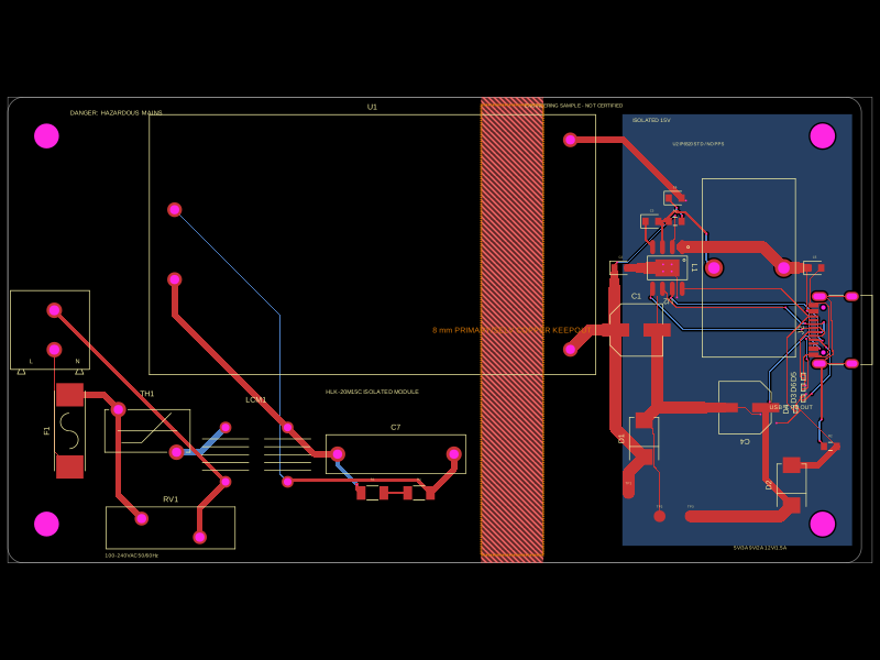 Similar packagetechmannih/usbc-chargerThis code defines a detailed electronic hardware design for an 85-265VAC to USB-C PD 18W wall charger, including the schematic layout and physical component placements such as connectors, filtering inductors, capacitors, resistors, protection diodes, and an isolated power module, all integrated with 3D models and mechanical enclosures.
 Discover something newimrishabh18/test-npmA compact electronic circuit consisting of a power input with diode protection, a decoupling capacitor, a pushbutton switch, a resistor, and a red LED indicator on a 40mm by 25mm PCB.