seveibar/usbc-pd-charger
This code defines and assembles a hardware schematic of an 18W USB-C PD wall charger with mains input, protection, high-voltage isolation, a DC buck converter with switching regulator, filtering, and USB-C output with ESD protection.
- Version
- 1.0.2
- License
- unset
- Stars
- 0
FABRICATION_CHECKLIST.md
# Fabrication and validation checklist

## Before ordering

- [ ] Open the Gerber ZIP in an independent viewer and confirm a 136 mm × 52 mm outline.
- [ ] Confirm the 8 mm primary/SELV corridor contains no top or bottom copper, vias, or plated holes.
- [ ] Confirm all mains traces are top-layer only and keep at least the intended several-millimetre separation between line and neutral.
- [ ] Verify every imported footprint against its current vendor drawing, especially J1 (TE 282838-2 / JLCPCB C5168775), PS1, U1, U2, Q1, J2, D2, and D3.
- [ ] Verify the USB-C receptacle contact order against LCSC C7431072; the imported labels required manual correction.
- [ ] Confirm the QFN-24 exposed-pad land pattern and stencil aperture with the STUSB4710A package drawing.
- [ ] Review U1 and U2 exposed-pad thermal conduction. This prototype routes both pads to ground, but a production spin should add a reviewed ground-plane/thermal-via pattern.
- [ ] Reconcile `annotated_bom.csv` with distributor stock and derating requirements.
- [ ] Prepare and verify the STUSB4710A NVM image before attaching a sink.

## Suggested PCB order

- Two-layer FR-4, 1.6 mm, UL-recognized laminate.
- 1 oz copper minimum; consider 2 oz after confirming the QFN and USB-C fine-pitch process.
- 0.10 mm minimum trace/space capability or better.
- 0.60 mm via pads with 0.30 mm finished drills.
- ENIG preferred for the USB-C/QFN prototype; lead-free HASL is acceptable only if the assembler approves the fine pitch.
- Soldermask on both sides; no copper pour added inside the marked isolation corridor.
- IPC Class 2 prototype workmanship at minimum.

## Assembly

- [ ] Hand/manual-review all mains-side through-hole parts and polarity/orientation.
- [ ] Use the approved 1 A / 250 V fuse and 14D471K MOV; do not substitute lower-voltage parts.
- [ ] Fit PS1 as the exact IRM-20-24 safety-approved module.
- [ ] Inspect QFN exposed-pad wetting and all USB-C contacts with X-ray or microscope as appropriate.
- [ ] Populate R12 for normal module-powered operation; depopulate it for isolated J4 injection.
- [ ] Clean flux residues, particularly across the isolation corridor.

## Low-voltage bring-up

- [ ] Keep J1 disconnected and R12 removed.
- [ ] Inject isolated 24 V at J4 with a 100 mA starting current limit.
- [ ] Check VIN24, 3V3, the STUSB internal 2.7 V/1.2 V rails, and the default ~5.02 V buck output.
- [ ] Program and read back the five PDOs through J3.
- [ ] Test 5/9/12/15/20 V negotiations with a PD analyzer and an electronic load.
- [ ] Measure startup/transition overshoot, ripple, VBUS discharge, and load-switch disconnect behavior.
- [ ] Run thermal tests at 5 V/3 A and 20 V/0.9 A, including hot ambient and blocked-convection conditions.

## Mains qualification — qualified personnel only

- [ ] Independent schematic/layout safety review.
- [ ] Flame-rated, touch-safe enclosure and approved cord/blade/terminal mechanics.
- [ ] Isolation transformer, fused test fixture, differential probes, and controlled access during first power-up.
- [ ] Hipot, leakage/touch current, protective impedance, abnormal operation, single-fault, and temperature-rise testing.
- [ ] Conducted/radiated emissions and immunity/surge testing.
- [ ] USB-C/USB-PD compliance testing.
- [ ] Applicable UL/ETL, FCC, and market-specific certification plan.

Stop immediately for unexpected input current, heating, odor, audible arcing, unstable VBUS, failed PD transitions, or any evidence of isolation-barrier contamination or damage.
Related Packages
 More from this authorseveibar/two-test-pointsA 10mm x 10mm circuit board with two test points connected by a trace.
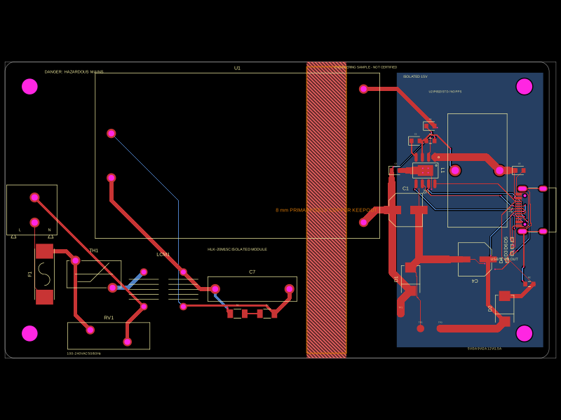 Similar packagetechmannih/usbc-chargerThis code defines a detailed electronic hardware design for an 85-265VAC to USB-C PD 18W wall charger, including the schematic layout and physical component placements such as connectors, filtering inductors, capacitors, resistors, protection diodes, and an isolated power module, all integrated with 3D models and mechanical enclosures.
 Discover something newimrishabh18/test-npmA compact electronic circuit consisting of a power input with diode protection, a decoupling capacitor, a pushbutton switch, a resistor, and a red LED indicator on a 40mm by 25mm PCB.