seveibar/usb-reseter
A tscircuit package created by seveibar.
- Version
- 1.1.4
- License
- unset
- Stars
- 0
lib/Passthrough.tsx
import { UsbC } from "./UsbC"
import { TPS22918DBVR } from "../imports/TPS22918DBVR"
import { A_2N7002 } from "../imports/A_2N7002"
import { PassthroughData } from "./PassthroughData"

const SECTION = "passthrough"

// USB 2.0 passthrough: data goes straight across (see PassthroughData), VBUS
// goes through a load switch. PWR_EN is pulled up to VBUS_IN so the output is on by default (even
// with no control USB attached); driving PWR_CUT high turns the output off.
export const Passthrough = () => (
  <>
    {/* Right edge: input from the host */}
    <UsbC
      name="J3"
      pcbX={15.3}
      pcbY={-10}
      pcbRotation={90}
      schSectionName={SECTION}
      connections={{
        VBUS1: "net.VBUS_IN",
        VBUS2: "net.VBUS_IN",
        GND1: "net.GND",
        GND2: "net.GND",
        SHELL1: "net.GND",
        SHELL2: "net.GND",
        SHELL3: "net.GND",
        SHELL4: "net.GND",
        DP1: "net.PT_DP",
        DP2: "net.PT_DP",
        DM1: "net.PT_DN",
        DM2: "net.PT_DN",
        CC1: "net.IN_CC1",
        CC2: "net.IN_CC2",
      }}
    />
    <resistor
      name="R8"
      resistance="5.1k"
      footprint="0402"
      schSectionName={SECTION}
      schOrientation="pos_top"
      pcbX={11}
      pcbY={-6}
      connections={{ pin1: "net.IN_CC2", pin2: "net.GND" }}
    />
    <resistor
      name="R9"
      resistance="5.1k"
      footprint="0402"
      schSectionName={SECTION}
      schOrientation="pos_top"
      pcbX={9.6}
      pcbY={-12.2}
      pcbRotation={180}
      connections={{ pin1: "net.IN_CC1", pin2: "net.GND" }}
    />

    {/* Left edge: switched output to the device */}
    <UsbC
      name="J2"
      pcbX={-15.3}
      pcbY={-10}
      pcbRotation={270}
      schSectionName={SECTION}
      connections={{
        VBUS1: "net.VBUS_OUT",
        VBUS2: "net.VBUS_OUT",
        GND1: "net.GND",
        GND2: "net.GND",
        SHELL1: "net.GND",
        SHELL2: "net.GND",
        SHELL3: "net.GND",
        SHELL4: "net.GND",
        DP1: "net.PT_DP",
        DP2: "net.PT_DP",
        DM1: "net.PT_DN",
        DM2: "net.PT_DN",
        CC1: "net.OUT_CC1",
        CC2: "net.OUT_CC2",
      }}
    />
    {/* 56k Rp to the switched VBUS: advertise default USB power, and vanish
        when the output is cut so the device sees a clean detach */}
    <resistor
      name="R10"
      resistance="56k"
      footprint="0402"
      schSectionName={SECTION}
      schOrientation="neg_top"
      pcbX={-9.6}
      pcbY={-13.4}
      connections={{ pin1: "net.OUT_CC1", pin2: "net.VBUS_OUT" }}
    />
    <resistor
      name="R11"
      resistance="56k"
      footprint="0402"
      schSectionName={SECTION}
      schOrientation="neg_top"
      pcbX={-9.6}
      pcbY={-12.2}
      connections={{ pin1: "net.OUT_CC2", pin2: "net.VBUS_OUT" }}
    />

    <PassthroughData />

    {/* VBUS load switch, 2A, with quick output discharge so the device
        actually loses power when cut */}
    <TPS22918DBVR
      name="U4"
      pcbX={5}
      pcbY={-15}
      schSectionName={SECTION}
      connections={{
        VIN: "net.VBUS_IN",
        GND: "net.GND",
        ON: "net.PWR_EN",
        CT: "net.PWR_CT",
        QOD: "net.VBUS_OUT",
        VOUT: "net.VBUS_OUT",
      }}
    />
    <capacitor
      name="C16"
      capacitance="10uF"
      footprint="0603"
      schSectionName={SECTION}
      maxDecouplingTraceLength={20}
      pcbX={9}
      pcbY={-15}
      pcbRotation={90}
      connections={{ pos: "net.VBUS_IN", neg: "net.GND" }}
    />
    <capacitor
      name="C17"
      capacitance="1uF"
      footprint="0402"
      schSectionName={SECTION}
      maxDecouplingTraceLength={20}
      pcbX={1.5}
      pcbY={-15}
      pcbRotation={90}
      connections={{ pos: "net.VBUS_OUT", neg: "net.GND" }}
    />
    {/* ~1ms VOUT rise time to limit inrush into the device */}
    <capacitor
      name="C18"
      capacitance="1nF"
      footprint="0402"
      schSectionName={SECTION}
      pcbX={5}
      pcbY={-12.4}
      connections={{ pos: "net.PWR_CT", neg: "net.GND" }}
    />

    <resistor
      name="R12"
      resistance="100k"
      footprint="0402"
      schSectionName={SECTION}
      schOrientation="neg_top"
      pcbX={7.5}
      pcbY={-11.4}
      connections={{ pin1: "net.PWR_EN", pin2: "net.VBUS_IN" }}
    />
    <A_2N7002
      name="Q1"
      pcbX={7.5}
      pcbY={-7.3}
      schSectionName={SECTION}
      connections={{ D: "net.PWR_EN", S: "net.GND", G: "net.PWR_CUT" }}
    />
    <resistor
      name="R13"
      resistance="100k"
      footprint="0402"
      schSectionName={SECTION}
      schOrientation="pos_top"
      pcbX={4.6}
      pcbY={-7.3}
      pcbRotation={90}
      connections={{ pin1: "net.PWR_CUT", pin2: "net.GND" }}
    />

    {/* VBUS sense dividers (5V -> 3.0V) into the RP2040 ADC */}
    <resistor
      name="R14"
      resistance="100k"
      footprint="0402"
      schSectionName={SECTION}
      schOrientation="pos_top"
      pcbX={11.1}
      pcbY={-15.6}
      pcbRotation={180}
      connections={{ pin1: "net.VBUS_IN", pin2: "net.VBUS_IN_SENSE" }}
    />
    <resistor
      name="R15"
      resistance="150k"
      footprint="0402"
      schSectionName={SECTION}
      schOrientation="pos_top"
      pcbX={10.7}
      pcbY={-16.7}
      connections={{ pin1: "net.VBUS_IN_SENSE", pin2: "net.GND" }}
    />
    <resistor
      name="R16"
      resistance="100k"
      footprint="0402"
      schSectionName={SECTION}
      schOrientation="pos_top"
      pcbX={-7.5}
      pcbY={-13}
      connections={{ pin1: "net.VBUS_OUT", pin2: "net.VBUS_OUT_SENSE" }}
    />
    <resistor
      name="R17"
      resistance="150k"
      footprint="0402"
      schSectionName={SECTION}
      schOrientation="pos_top"
      pcbX={-7.5}
      pcbY={-14.2}
      pcbRotation={180}
      connections={{ pin1: "net.VBUS_OUT_SENSE", pin2: "net.GND" }}
    />
  </>
)
Related Packages
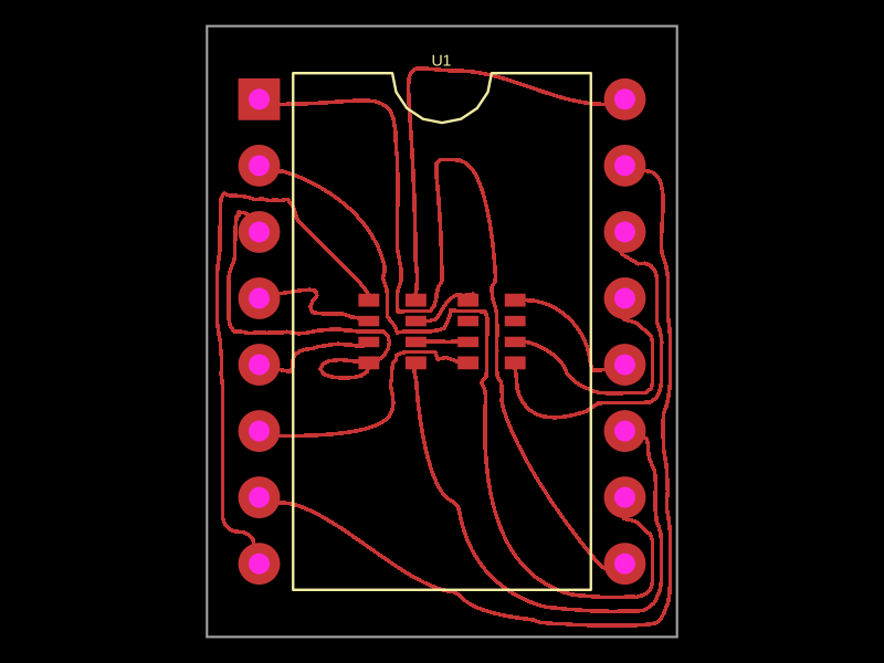 More from this authorseveibar/single-layer-tdA single-chip DIP-16 package circuit connecting pins 1–8 to corresponding internal pins 9–16.
 Discover something new0hmX/am3352-ddr-track-c-stackup-wip-20261007Saved native stackup-first preview: 11 DDR endpoint routes and 179 selected pad-to-plane joins. Matching and full-board connectivity incomplete. Not fabrication-ready.