seveibar/pedometer
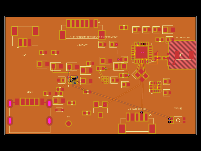
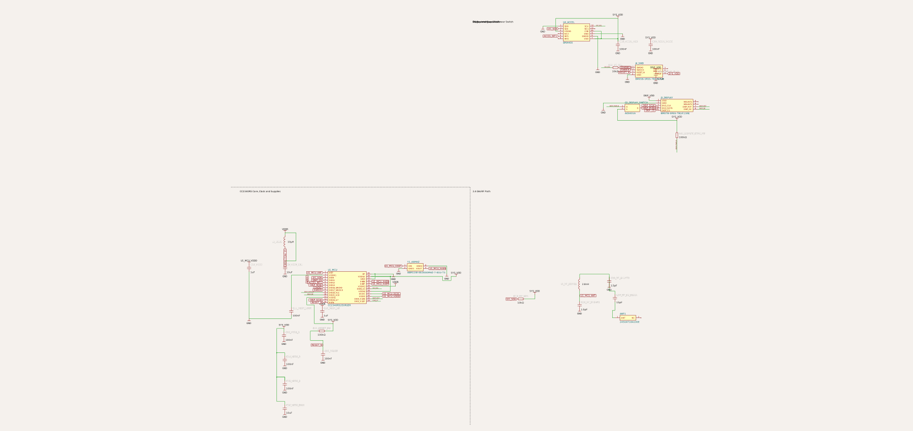
This hardware setup integrates a Type-C connector, battery, display, and RF antenna connected through a microcontroller, USB interface, charging and fuel gauge ICs, along with associated passive components, enabling power management, data communication, and signal processing.
- Version
- 0.4.4
- License
- unset
- Stars
- 1
index.circuit.tsx
PCB
Schematic
import { A_1TS026A_1600_0553_CT } from "./imports/A_1TS026A_1600_0553_CT"
import { A_2450AT18A100E } from "./imports/A_2450AT18A100E"
import { ABM11W_48_0000MHZ_7_B1U_T3 } from "./imports/ABM11W_48_0000MHZ_7_B1U_T3"
import { AO3401A } from "./imports/AO3401A"
import { BMA400 } from "./imports/BMA400"
import { BM03B_SRSS_TB_LF__SN_ } from "./imports/BM03B_SRSS_TB_LF__SN_"
import { BM05B_SRSS_TB_LF__SN_ } from "./imports/BM05B_SRSS_TB_LF__SN_"
import { BM07B_SRSS_TB_LF__SN_ } from "./imports/BM07B_SRSS_TB_LF__SN_"
import { BQ25150YFPR } from "./imports/BQ25150YFPR"
import { BQ27427YZFR } from "./imports/BQ27427YZFR"
import { CC2340R52E0RGER } from "./imports/CC2340R52E0RGER"
import { ESD5Z5_0T1G } from "./imports/ESD5Z5_0T1G"
import { TYPE_C_6PIN } from "./imports/TYPE_C_6PIN"

const r0402 = {
  "0": { jlcpcb: ["C22356212"] },
  "5k1": { jlcpcb: ["C25905"] },
  "10k": { jlcpcb: ["C25744"] },
  "100k": { jlcpcb: ["C25741"] },
}

const c0402 = {
  "1p5": { jlcpcb: ["C76901"] },
  "100n": { jlcpcb: ["C1525"] },
  "1u": { jlcpcb: ["C5137473"] },
  "2u2": { jlcpcb: ["C12530"] },
}

const c0603 = {
  "2u2": { jlcpcb: ["C1607"] },
  "4u7": { jlcpcb: ["C1705"] },
  "10u": { jlcpcb: ["C19702"] },
}

// Numeric pcbPath points below are local to the first component, including its rotation.
// Compact 0402 RF lands: 0.50 x 0.50 mm pads, 1.00 mm pitch; courtyard includes 0.10 mm land margin.
const rf0402 = <footprint>
  <smtpad portHints={["pin1"]} pcbX={-0.5} pcbY={0} width={0.5} height={0.5} shape="rect" />
  <smtpad portHints={["pin2"]} pcbX={0.5} pcbY={0} width={0.5} height={0.5} shape="rect" />
  <courtyardoutline outline={[{x:-0.85,y:-0.35},{x:0.85,y:-0.35},{x:0.85,y:0.35},{x:-0.85,y:0.35},{x:-0.85,y:-0.35}]} />
</footprint>

const PowerTrace = (props: any) => <trace {...props} schSheetName="power" />
const LogicTrace = (props: any) => <trace {...props} schSheetName="logic" />

export default () => (
  <board
    name="PedometerBoard"
    title="BLE Pedometer — CC2340R5 / BQ25150 / BQ27427 / BMA400"
    width="42mm"
    height="26mm"
    layers={4}
    allowBlindAndBuriedVias
    thickness="1mm"
    solderMaskColor="black"
    minTraceWidth="0.1mm"
    defaultTraceWidth="0.12mm"
    minViaHoleDiameter="0.1mm"
    minViaPadDiameter="0.2mm"
    minTraceToPadEdgeClearance="0.05mm"
    minViaEdgeToPadEdgeClearance="0.05mm"
    minPadEdgeToPadEdgeClearance="0.05mm"
    minBoardEdgeClearance="0.15mm"
    autorouterVersion="beta_pipeline9"
    autorouterEffortLevel="100x"
    autorouter={{ preset: "auto_local", allowViaInPad: true, traceClearance: "0.1mm" }}
    pcbStyle={{ silkscreenTextVisibility: "hidden", viaHoleDiameter: 0.1, viaPadDiameter: 0.2 }}
    schAutoLayoutEnabled
  >
    <schematicsheet name="power" displayName="Power Management" sheetIndex={0} sheetSize="ANSI_B">
      <schematicsection name="power_input" displayName="USB-C Input and Protection" />
      <schematicsection name="charger" displayName="Charger, Battery and Power Path" />
      <schematicsection name="gauge" displayName="Fuel Gauge" />
    </schematicsheet>
    <schematicsheet name="logic" displayName="BLE, Sensors and Display" sheetIndex={1} sheetSize="ANSI_B" sheetWidth="520mm">
      <schematicsection name="logic_core" displayName="CC2340R5 Core, Clock and Supplies" />
      <schematicsection name="sensors" displayName="I2C Bus and Step Sensor" />
      <schematicsection name="display" displayName="Display Interface and Power Switch" />
      <schematicsection name="rf" displayName="2.4 GHz RF Path" />
      <schematicsection name="debug" displayName="Programming and Test" />
    </schematicsheet>


    <net name="SWDIO" />
    <net name="SWDCK" />
    <net name="RESET_N" />


    <net name="ACCEL_INT1" />
    <net name="I2C_SCL" />
    <net name="I2C_SDA" />


    <net name="DISP_MOSI" />

    <net name="VDDR" />


    <net name="CHG_LP" />


    {/* External interfaces */}
    <TYPE_C_6PIN name="J1_USB_C" pcbX={-15.5} pcbY={-7.5} schSheetName="power" schSectionName="power_input" schWidth={1.77} schHeight={1.2} />
    <BM03B_SRSS_TB_LF__SN_ name="J2_BATTERY" pcbX={-16.5} pcbY={8.5} pcbRotation={180} schSheetName="power" schSectionName="charger" schWidth={2.2} schHeight={0.6} schX={-3.95} schY={-2.75} />
    <BM07B_SRSS_TB_LF__SN_ name="J3_DISPLAY" pcbX={-4.0} pcbY={10.0} schSheetName="logic" schSectionName="display" schWidth={2.6} schHeight={1.0} schX={8.1} schY={-5.89} />

    {/* USB-C sink configuration and input protection */}
    <resistor name="R1_CC1" resistance="5.1kohm" footprint="0402" supplierPartNumbers={r0402["5k1"]} pcbX={-11.6} pcbY={-4.0} schSheetName="power" schSectionName="power_input" />
    <resistor name="R2_CC2" resistance="5.1kohm" footprint="0402" supplierPartNumbers={r0402["5k1"]} pcbX={-9.2} pcbY={-4.0} pcbRotation={180} schSheetName="power" schSectionName="power_input" />
    <ESD5Z5_0T1G name="D1_VBUS_TVS" symbol={undefined} pcbX={-9.0} pcbY={-7.5} schSheetName="power" schSectionName="power_input" />
    <capacitor name="C1_VBUS" capacitance="4.7uF" footprint="0603" supplierPartNumbers={c0603["4u7"]} pcbX={-9.0} pcbY={-5.5} schSheetName="power" schSectionName="power_input" schOrientation="vertical" />

    {/* Charger / PMIC */}
    <group name="charger_region" pcbX={-6} pcbY={-1}>
    <BQ25150YFPR name="U2_CHARGER" pcbX={0} pcbY={0} schSheetName="power" schSectionName="charger" schWidth={1.58} schHeight={2.2} schX={-4.49} schY={-6.57} />
    <capacitor name="C2_PMID" capacitance="10uF" footprint="0603" supplierPartNumbers={c0603["10u"]} pcbX={-3.5} pcbY={3.0} schSheetName="power" schSectionName="charger" schOrientation="vertical" />
    <capacitor name="C3_VINLS" capacitance="4.7uF" footprint="0603" supplierPartNumbers={c0603["4u7"]} pcbX={0.0} pcbY={2.9} schSheetName="power" schSectionName="charger" schOrientation="vertical" />
    <A_1TS026A_1600_0553_CT name="SW1_WAKE" schX={-2.35} schY={-9.79} pcbX={23.0} pcbY={-8.8} schSheetName="power" schSectionName="charger" />
    </group>
    <capacitor name="C4_VSYS_SENSE" capacitance="1uF" footprint="0402" supplierPartNumbers={c0402["1u"]} pcbX={-8.7} pcbY={-1.0} pcbRotation={180} schSheetName="power" schSectionName="charger" schOrientation="vertical" />
    <capacitor name="C5_CHG_VDD" capacitance="4.7uF" footprint="0603" supplierPartNumbers={c0603["4u7"]} pcbX={-3.0} pcbY={-1.2} schSheetName="power" schSectionName="charger" schOrientation="vertical" />
    <capacitor name="C6_SYS_VDD" capacitance="4.7uF" footprint="0603" supplierPartNumbers={c0603["4u7"]} pcbX={-3.0} pcbY={1.1} schSheetName="power" schSectionName="charger" schOrientation="vertical" schX={-5.48} schY={-8.86} />
    <resistor name="R3_IMAX" resistance="10kohm" footprint="0402" supplierPartNumbers={r0402["10k"]} pcbX={-8.8} pcbY={-3.0} schSheetName="power" schSectionName="charger" schX={-3.8} schY={-9.44} />
    <resistor name="R4_TS_BIAS" resistance="10kohm" footprint="0402" supplierPartNumbers={r0402["10k"]} pcbX={-12.5} pcbY={5.0} schSheetName="power" schSectionName="charger" />
    <resistor name="R5_TS_NO_NTC" resistance="10kohm" footprint="0402" supplierPartNumbers={r0402["10k"]} doNotPlace pcbX={-9.8} pcbY={5.0} schSheetName="power" schSectionName="charger" schX={-6.83} schY={-2.15} />
    <resistor name="R7_LP_BOOT_PD" resistance="100kohm" footprint="0402" supplierPartNumbers={r0402["100k"]} pcbX={-2.8} pcbY={-3.6} schSheetName="power" schSectionName="charger" />
    <resistor name="R8_PG_PU" resistance="100kohm" footprint="0402" supplierPartNumbers={r0402["100k"]} pcbX={-6.3} pcbY={-6.0} schSheetName="power" schSectionName="charger" schX={-9.026} schY={-8.785} />

    {/* Fuel gauge. BAT is the cell side; SRX is the system/charger side. */}
    <group name="gauge_region" pcbX={1} pcbY={-1}>
    <BQ27427YZFR name="U3_GAUGE" pcbX={0} pcbY={0} schSheetName="power" schSectionName="gauge" schWidth={1.58} schHeight={1.0} />
    <resistor name="R10_GAUGE_INT_PU" doNotPlace resistance="10kohm" footprint="0402" supplierPartNumbers={r0402["10k"]} pcbX={-1.0} pcbY={2.5} schSheetName="power" schSectionName="gauge" schX={13.707} schY={-4.464} />
    <resistor name="R12_I2C_SCL" resistance="10kohm" footprint="0402" supplierPartNumbers={r0402["10k"]} pcbX={4.0} pcbY={1.0} schSheetName="logic" schSectionName="sensors" />
    </group>
    <capacitor name="C7_GAUGE_BAT" capacitance="1uF" footprint="0402" supplierPartNumbers={c0402["1u"]} pcbX={5.6} pcbY={-2.0} schSheetName="power" schSectionName="gauge" schOrientation="vertical" />
    <capacitor name="C8_GAUGE_VDD" capacitance="2.2uF" footprint="0402" supplierPartNumbers={c0402["2u2"]} pcbX={3.2} pcbY={-1.0} schSheetName="power" schSectionName="gauge" schOrientation="vertical" />
    <resistor name="R9_BIN_PD" resistance="10kohm" footprint="0402" supplierPartNumbers={r0402["10k"]} pcbX={-2.2} pcbY={2.6} schSheetName="power" schSectionName="gauge" />

    {/* Wireless MCU, clocks, and TI reference power network */}
    <group name="mcu_region" pcbX={9} pcbY={5}>
    <CC2340R52E0RGER name="U1_MCU" pcbX={0} pcbY={0} pcbRotation={180} schSheetName="logic" schSectionName="logic_core" schWidth={3.1} schHeight={2.6} schX={-18.5} schY={-20.58} />
    {/* Five-pin JST-SH programming connector. VTREF is a sense output, not power input. */}
    <BM05B_SRSS_TB_LF__SN_ name="J4_SWD" pcbX={-1.0} pcbY={-15.4} schSheetName="logic" schSectionName="debug" schWidth={2.2} schHeight={1.0}
      connections={{ SWDIO: "net.SWDIO", SWDCK: "net.SWDCK", RESET_N: "net.RESET_N", GND: "net.GND", VTREF: "net.SYS_VDD" }} />
    <AO3401A name="Q1_DISPLAY_SWITCH" symbol={undefined} pcbX={-9.0} pcbY={-12.5} pcbRotation={90} schSheetName="logic" schSectionName="display" schX={4.5} schY={-6.09} />
    <ABM11W_48_0000MHZ_7_B1U_T3 name="Y1_48MHZ" symbol={undefined} pcbX={0} pcbY={-5.0} pcbRotation={315} schSheetName="logic" schSectionName="logic_core" schX={-13.0} schY={-18.94} />
    </group>
    <inductor name="L1_DCDC" inductance="10uH" footprint="0603" supplierPartNumbers={{ jlcpcb: ["C713281"] }} pcbX={4.3} pcbY={2.0} schSheetName="logic" schSectionName="logic_core" />
    <capacitor name="C9_VDDR_10U" capacitance="10uF" footprint="0603" supplierPartNumbers={c0603["10u"]} pcbX={1.3} pcbY={3.2} schSheetName="logic" schSectionName="logic_core" schOrientation="vertical" schX={-23.5} schY={-19.0} />
    <capacitor name="C10_VDDR_1U" capacitance="1uF" footprint="0402" supplierPartNumbers={c0402["1u"]} pcbX={0.5} pcbY={6.8} schSheetName="logic" schSectionName="logic_core" schOrientation="vertical" schX={-20.5} schY={-22.5} />
    <capacitor name="C11_VDDR_100N" capacitance="100nF" footprint="0402" supplierPartNumbers={c0402["100n"]} pcbX={3.0} pcbY={6.8} schSheetName="logic" schSectionName="logic_core" schOrientation="vertical" schX={-23.0} schY={-22.5} />
    <capacitor name="C12_VDDD" pcbRotation={180} capacitance="1uF" footprint="0402" supplierPartNumbers={c0402["1u"]} pcbX={5.0} pcbY={3.5} schSheetName="logic" schSectionName="logic_core" schOrientation="vertical" />
    <capacitor name="C13_VDDS_1" capacitance="100nF" footprint="0402" supplierPartNumbers={c0402["100n"]} pcbX={8.0} pcbY={10.0} schSheetName="logic" schSectionName="logic_core" schOrientation="vertical" />
    <capacitor name="C14_VDDS_2" capacitance="100nF" footprint="0402" supplierPartNumbers={c0402["100n"]} pcbX={10.2} pcbY={10.0} schSheetName="logic" schSectionName="logic_core" schOrientation="vertical" />
    <capacitor name="C15_VDDS_3" capacitance="100nF" footprint="0402" supplierPartNumbers={c0402["100n"]} pcbX={12.4} pcbY={10.0} schSheetName="logic" schSectionName="logic_core" schOrientation="vertical" />
    <capacitor name="C16_VDDS_BULK" capacitance="10uF" footprint="0603" supplierPartNumbers={c0603["10u"]} pcbX={15.0} pcbY={10.0} schSheetName="logic" schSectionName="logic_core" schOrientation="vertical" />
    <resistor name="R11_RESET_PU" resistance="100kohm" footprint="0402" supplierPartNumbers={r0402["100k"]} pcbX={13.0} pcbY={7.8} schSheetName="logic" schSectionName="logic_core" schX={-20.544} schY={-24.087} />
    <capacitor name="C17_RESET" capacitance="100nF" footprint="0402" supplierPartNumbers={c0402["100n"]} pcbX={15.3} pcbY={7.8} schSheetName="logic" schSectionName="logic_core" schOrientation="vertical" />

    {/* BMA400 hardware step counter */}
    <group name="sensor_region" pcbX={12} pcbY={-2.5}>
    <BMA400 name="U4_ACCEL" pcbX={0} pcbY={0} schSheetName="logic" schSectionName="sensors" schWidth={2.15} schHeight={1.4} />
    <capacitor name="C18_ACCEL_VDD" capacitance="100nF" footprint="0402" supplierPartNumbers={c0402["100n"]} pcbX={2.7} pcbY={1.2} schSheetName="logic" schSectionName="sensors" schOrientation="vertical" />
    <capacitor name="C19_ACCEL_VDDIO" capacitance="100nF" footprint="0402" supplierPartNumbers={c0402["100n"]} pcbX={2.7} pcbY={-1.3} schSheetName="logic" schSectionName="sensors" schOrientation="vertical" />
    </group>

    {/* Management I2C pull-ups. OLED uses separate SPI pins to avoid back-power. */}
    <resistor name="R13_I2C_SDA" resistance="10kohm" footprint="0402" supplierPartNumbers={r0402["10k"]} pcbX={5.1} pcbY={10.5} schSheetName="logic" schSectionName="sensors" />
    <capacitor name="C20_DISPLAY_BULK" capacitance="4.7uF" footprint="0603" supplierPartNumbers={c0603["4u7"]} pcbX={-12.5} pcbY={2.5} schSheetName="logic" schSectionName="display" schOrientation="vertical" />
    <resistor name="R15_DISPLAY_GATE_PU" resistance="100kohm" footprint="0402" supplierPartNumbers={r0402["100k"]} pcbX={-3.0} pcbY={-8.2} schSheetName="logic" schSectionName="display" />

    {/* TI reference RF match followed by a board/enclosure tuning section. */}
    <capacitor name="C21_RF_SHUNT1" capacitance="1.5pF" footprint={rf0402} supplierPartNumbers={c0402["1p5"]} pcbX={12.05} pcbY={4.25} pcbRotation={90} schSheetName="logic" schSectionName="rf" schOrientation="vertical" />
    <inductor name="L2_RF_SERIES" inductance="2.8nH" footprint={rf0402} pcbX={13.4} pcbY={3.75} pcbRotation={0} schSheetName="logic" schSectionName="rf" />
    <capacitor name="C22_RF_SHUNT2" capacitance="1.5pF" footprint={rf0402} supplierPartNumbers={c0402["1p5"]} pcbX={14.75} pcbY={4.25} pcbRotation={90} schSheetName="logic" schSectionName="rf" schOrientation="vertical" />
    <capacitor name="C24_RF_DC_BLOCK" schOrientation="vertical" capacitance="15pF" footprint={rf0402} pcbX={15.5} pcbY={2.5} pcbRotation={0} schSheetName="logic" schSectionName="rf" />
    <A_2450AT18A100E name="ANT1" symbol={undefined} pcbX={18.3} pcbY={4.5} pcbRotation={0} schSheetName="logic" schSectionName="rf" />
    <keepout
      shape="rect"
      width="6mm"
      height="6mm"
      pcbX={18.0}
      pcbY={4.5}
      layers={["inner1", "inner2", "bottom"]}
      excludeRefs={[".ANT1"]}
    />
    <silkscreentext text="ANT KEEP-OUT" pcbX={18.0} pcbY={8.3} fontSize="0.45mm" anchorAlignment="center" pcbStyle={{ silkscreenTextVisibility: "visible" }} />

    <testpoint name="TP6_PG" footprintVariant="pad" padDiameter="1.0mm" pcbX={-7.0} pcbY={-10.5} connections={{ pin1: "net.CHG_PG" }} schSheetName="power" schSectionName="charger" />

    {/* Deliberately sparse, legible production silkscreen. */}
    <silkscreentext text="USB" pcbX={-15.5} pcbY={-3.6} fontSize="0.6mm" anchorAlignment="center" pcbStyle={{ silkscreenTextVisibility: "visible" }} />
    <silkscreentext text="BAT" pcbX={-16.5} pcbY={4.5} fontSize="0.6mm" anchorAlignment="center" pcbStyle={{ silkscreenTextVisibility: "visible" }} />
    <silkscreentext text="DISPLAY" pcbX={-4.0} pcbY={6.7} fontSize="0.6mm" anchorAlignment="center" pcbStyle={{ silkscreenTextVisibility: "visible" }} />
    <silkscreentext text="WAKE" pcbX={17.0} pcbY={-7.2} fontSize="0.55mm" anchorAlignment="center" pcbStyle={{ silkscreenTextVisibility: "visible" }} />
    <silkscreentext text="J4 SWD JST-SH" pcbX={8.0} pcbY={-7.3} fontSize="0.5mm" anchorAlignment="center" pcbStyle={{ silkscreenTextVisibility: "visible" }} />
    <silkscreentext text="PG" pcbX={-7.0} pcbY={-9.0} fontSize="0.4mm" anchorAlignment="center" pcbStyle={{ silkscreenTextVisibility: "visible" }} />
    <silkscreentext text="BLE PEDOMETER REV D EXPERIMENT" pcbX={-1.5} pcbY={8.4} fontSize="0.55mm" anchorAlignment="center" pcbStyle={{ silkscreenTextVisibility: "visible" }} />

    {/* USB-C and charging input connections */}
    <PowerTrace from=".J1_USB_C > .VBUS1" to="net.VBUS" width="0.15mm" />
    <PowerTrace from=".J1_USB_C > .VBUS2" to="net.VBUS" width="0.15mm" />
    <PowerTrace from=".J1_USB_C > .GND1" to=".J1_USB_C > .EH3" connectsTo="net.GND" width="0.15mm" pcbStraightLine />
    <PowerTrace from=".J1_USB_C > .GND2" to=".J1_USB_C > .EH4" connectsTo="net.GND" width="0.15mm" pcbStraightLine />
    <PowerTrace from=".J1_USB_C > .EH1" to="net.GND" width="0.15mm" />
    <PowerTrace from=".J1_USB_C > .EH2" to="net.GND" width="0.15mm" />
    <PowerTrace from=".J1_USB_C > .EH3" to="net.GND" width="0.15mm" />
    <PowerTrace from=".J1_USB_C > .EH4" to="net.GND" width="0.15mm" />
    <PowerTrace from=".J1_USB_C > .CC1" to=".R1_CC1 > .pin1" />
    <PowerTrace from=".R1_CC1 > .pin2" to="net.GND" />
    <PowerTrace from=".J1_USB_C > .CC2" to=".R2_CC2 > .pin1" />
    <PowerTrace from=".R2_CC2 > .pin2" to="net.GND" />
    <PowerTrace from=".D1_VBUS_TVS > .C" to="net.VBUS" />
    <PowerTrace from=".D1_VBUS_TVS > .A" to="net.GND" />
    <PowerTrace from=".C1_VBUS > .pin1" to="net.VBUS" />
    <PowerTrace from=".C1_VBUS > .pin2" to="net.GND" />

    {/* Charger power and control. CE left open (internal enable pull-down); ADCIN unused/open per datasheet. */}
    <PowerTrace from=".U2_CHARGER > .IN" to="net.VBUS" width="0.15mm" />
    <PowerTrace from=".U2_CHARGER > .PMID1" to="net.PMID" width="0.1mm" />
    <PowerTrace from=".U2_CHARGER > .PMID2" to=".U2_CHARGER > .PMID1" connectsTo="net.PMID" width="0.1mm" pcbStraightLine />
    <PowerTrace from=".C2_PMID > .pin1" to=".C3_VINLS > .pin1" connectsTo="net.PMID" width="0.15mm" pcbPath={[".C2_PMID > .pin1", {x:-0.825,y:-1.2}, {x:2.675,y:-1.2}, ".C3_VINLS > .pin1"]} />
    <PowerTrace from=".C2_PMID > .pin2" to="net.GND" />
    <PowerTrace from=".U2_CHARGER > .VINLS" to=".U2_CHARGER > .PMID2" connectsTo="net.PMID" width="0.1mm" pcbPath={[".U2_CHARGER > .VINLS", {x:0.8001,y:0.599948}, {x:0.8001,y:0.599948,via:true,toLayer:"inner2"}, {x:0.8001,y:0.599948}, {x:0.8001,y:0.85}, {x:-0.40005,y:0.85}, {x:-0.40005,y:-0.199898}, {x:-0.40005,y:-0.199898,via:true,toLayer:"top"}, {x:-0.40005,y:-0.199898}, ".U2_CHARGER > .PMID2"]} />
    <PowerTrace from=".C3_VINLS > .pin1" to=".U2_CHARGER > .PMID1" connectsTo="net.PMID" width="0.15mm" pcbPath={[".C3_VINLS > .pin1", {x:-0.825,y:0}, {x:-0.825,y:0,via:true,toLayer:"inner1"}, {x:-0.825,y:0}, {x:-0.8001,y:-3.099898}, {x:-0.8001,y:-3.099898,via:true,toLayer:"top"}, {x:-0.8001,y:-3.099898}, ".U2_CHARGER > .PMID1"]} />
    <PowerTrace from=".C3_VINLS > .pin2" to=".U2_CHARGER > .GND" connectsTo="net.GND" width="0.12mm" pcbPath={[".C3_VINLS > .pin2", {x:0.825,y:0}, {x:0.825,y:0,via:true,toLayer:"bottom"}, {x:0.825,y:0}, {x:-1.15,y:-2.300052}, {x:-1.15,y:-2.300052,via:true,toLayer:"top"}, {x:-1.15,y:-2.300052}, ".U2_CHARGER > .GND"]} />
    <PowerTrace from=".U2_CHARGER > .BAT1" to="net.VSYS" width="0.1mm" />
    <PowerTrace from=".U2_CHARGER > .BAT2" to=".U2_CHARGER > .BAT1" connectsTo="net.VSYS" width="0.1mm" pcbStraightLine />
    <PowerTrace from=".C4_VSYS_SENSE > .pin1" to="net.VSYS" />
    <PowerTrace from=".C4_VSYS_SENSE > .pin2" to="net.GND" />
    <PowerTrace from=".U2_CHARGER > .VDD" to=".C5_CHG_VDD > .pin1" connectsTo="net.CHG_VDD_1V8" width="0.1mm" maxLength="10mm" pcbPath={[".U2_CHARGER > .VDD", {x:0.40005,y:-0.599948}, {x:0.40005,y:-0.599948,via:true,toLayer:"inner2"}, {x:0.40005,y:-0.599948}, {x:2.14,y:-0.2}, {x:2.14,y:-0.2,via:true,toLayer:"top"}, {x:2.14,y:-0.2}, ".C5_CHG_VDD > .pin1"]} />
    <PowerTrace from=".C5_CHG_VDD > .pin1" to="net.CHG_VDD_1V8" maxLength="10mm" />
    <PowerTrace from=".C5_CHG_VDD > .pin2" to="net.GND" maxLength="10mm" />
    <PowerTrace from=".U2_CHARGER > .LSLDO" to="net.SYS_VDD" width="0.1mm" pcbRouteHints={[{ x: -5.6, y: -0.4, via: true, to_layer: "bottom" }]} />
    <PowerTrace from=".C6_SYS_VDD > .pin1" to="net.SYS_VDD" />
    <PowerTrace from=".C6_SYS_VDD > .pin2" to="net.GND" />
    <PowerTrace from=".U2_CHARGER > .VIO" to="net.SYS_VDD" />
    <PowerTrace from=".U2_CHARGER > .GND" to="net.GND" />
    <PowerTrace from=".U2_CHARGER > .IMAX" to=".R3_IMAX > .pin1" width="0.1mm" maxLength="10mm" pcbPath={[".U2_CHARGER > .IMAX", {x:0.0,y:0.199898}, {x:0.0,y:0.199898,via:true,toLayer:"bottom"}, {x:0.0,y:0.199898}, {x:-3.31,y:-2.0}, {x:-3.31,y:-2.0,via:true,toLayer:"top"}, {x:-3.31,y:-2.0}, ".R3_IMAX > .pin1"]} />
    <PowerTrace from=".R3_IMAX > .pin2" to="net.GND" />
    <PowerTrace from=".U2_CHARGER > .TS" to="net.BATT_NTC" width="0.1mm" pcbRouteHints={[{ x: -6.4, y: -0.4, via: true, to_layer: "bottom" }]} />
    <PowerTrace from=".R4_TS_BIAS > .pin1" to="net.BATT_NTC" />
    <PowerTrace from=".R4_TS_BIAS > .pin2" to="net.GND" />
    <PowerTrace from=".R5_TS_NO_NTC > .pin1" to="net.BATT_NTC" />
    <PowerTrace from=".R5_TS_NO_NTC > .pin2" to="net.GND" />
    <PowerTrace from=".U2_CHARGER > .LP" to=".R7_LP_BOOT_PD > .pin1" connectsTo="net.CHG_LP" width="0.1mm" maxLength="10mm" pcbPath={[".U2_CHARGER > .LP", {x:0.40005,y:0.199898}, {x:0.40005,y:0.199898,via:true,toLayer:"bottom"}, {x:0.40005,y:0.199898}, {x:2.69,y:-2.6}, {x:2.69,y:-2.6,via:true,toLayer:"top"}, {x:2.69,y:-2.6}, ".R7_LP_BOOT_PD > .pin1"]} />
    <PowerTrace from=".R7_LP_BOOT_PD > .pin1" to="net.CHG_LP" />
    <PowerTrace from=".R7_LP_BOOT_PD > .pin2" to="net.GND" />
    <PowerTrace from=".U2_CHARGER > .PG" to="net.CHG_PG" width="0.1mm" pcbRouteHints={[{ x: -6.4, y: -1.6, via: true, to_layer: "bottom" }]} />
    <PowerTrace from=".R8_PG_PU > .pin1" to="net.CHG_PG" />
    <PowerTrace from=".R8_PG_PU > .pin2" to="net.SYS_VDD" />
    <PowerTrace from=".U2_CHARGER > .SCL" to="net.I2C_SCL" width="0.1mm" />
    <PowerTrace from=".U2_CHARGER > .SDA" to="net.I2C_SDA" />
    <PowerTrace from=".U2_CHARGER > .MR" to=".SW1_WAKE > .pin1" connectsTo="net.WAKE_MR_N" width="0.1mm" pcbPath={[".U2_CHARGER > .MR", {x:0,y:-0.599948}, {x:0,y:-0.599948,via:true,toLayer:"inner1"}, {x:0,y:-0.599948}, {x:0,y:-1.3}, {x:21.675009,y:-8.424969}, {x:21.675009,y:-8.424969,via:true,toLayer:"top"}, {x:21.675009,y:-8.424969}, ".SW1_WAKE > .pin1"]} />
    <PowerTrace from=".SW1_WAKE > .pin1" to="net.WAKE_MR_N" />
    <PowerTrace from=".SW1_WAKE > .pin2" to=".SW1_WAKE > .pin1" connectsTo="net.WAKE_MR_N" width="0.1mm" pcbPath={[".SW1_WAKE > .pin2", {x:-1.9,y:-0.375031}, {x:-1.9,y:-0.375031,via:true,toLayer:"bottom"}, {x:-1.9,y:-0.375031}, {x:-1.9,y:0.375031}, {x:-1.9,y:0.375031,via:true,toLayer:"top"}, {x:-1.9,y:0.375031}, ".SW1_WAKE > .pin1"]} />
    <PowerTrace from=".SW1_WAKE > .pin3" to="net.GND" />
    <PowerTrace from=".SW1_WAKE > .pin4" to="net.GND" />

    {/* Battery and integrated-sense-resistor fuel gauge */}
    <PowerTrace from=".J2_BATTERY > .BATTERY_POS" to="net.BAT_CELL" width="0.15mm" />
    <PowerTrace from=".J2_BATTERY > .NTC" to="net.BATT_NTC" />
    <PowerTrace from=".J2_BATTERY > .GND" to="net.GND" width="0.15mm" />
    <PowerTrace from=".U3_GAUGE > .BAT" to="net.BAT_CELL" width="0.15mm" />
    <PowerTrace from=".U3_GAUGE > .SRX" to="net.VSYS" width="0.15mm" />
    <PowerTrace from=".U3_GAUGE > .VSS1" to="net.GND" />
    <PowerTrace from=".U3_GAUGE > .VSS2" to="net.GND" />
    <PowerTrace from=".U3_GAUGE > .BIN" to=".R9_BIN_PD > .pin1" />
    <PowerTrace from=".R9_BIN_PD > .pin2" to="net.GND" />
    <PowerTrace from=".U3_GAUGE > .BAT" to=".C7_GAUGE_BAT > .pin1" />
    <PowerTrace from=".C7_GAUGE_BAT > .pin2" to="net.GND" />
    <PowerTrace from=".U3_GAUGE > .VDD" to=".C8_GAUGE_VDD > .pin1" maxLength="10mm" />
    <PowerTrace from=".C8_GAUGE_VDD > .pin2" to="net.GND" maxLength="10mm" pcbRouteHints={[{ x: 3.71, y: -1.0, via: true, to_layer: "bottom" }]} />
    <PowerTrace from=".U3_GAUGE > .SCL" to="net.I2C_SCL" width="0.1mm" />
    <PowerTrace from=".U3_GAUGE > .SDA" to=".U4_ACCEL > .SDX" connectsTo="net.I2C_SDA" width="0.1mm" />
    <PowerTrace from=".U3_GAUGE > .GPOUT" to=".R10_GAUGE_INT_PU > .pin1" connectsTo="net.GAUGE_INT_N" width="0.1mm" pcbStraightLine />
    <PowerTrace from=".R10_GAUGE_INT_PU > .pin1" to="net.GAUGE_INT_N" />
    <PowerTrace from=".R10_GAUGE_INT_PU > .pin2" to="net.SYS_VDD" />

    {/* MCU power, clock, SWD and GPIO */}
    <LogicTrace from=".U1_MCU > .VDDS1" to="net.SYS_VDD" width="0.12mm" />
    <LogicTrace from=".U1_MCU > .VDDS2" to=".U1_MCU > .VDDS1" connectsTo="net.SYS_VDD" width="0.12mm" pcbPath={[".U1_MCU > .VDDS2", {x:1.89992,y:1.250061}, {x:1.89992,y:1.250061,via:true,toLayer:"inner2"}, {x:1.89992,y:1.250061}, {x:0.7498,y:-2.05}, {x:0.7498,y:-2.05,via:true,toLayer:"top"}, {x:0.7498,y:-2.05}, ".U1_MCU > .VDDS1"]} />
    <LogicTrace from=".U1_MCU > .VDDS3" to=".U1_MCU > .VDDS1" connectsTo="net.SYS_VDD" width="0.12mm" pcbPath={[".U1_MCU > .VDDS3", {x:-1.250188,y:1.900047}, {x:-1.250188,y:1.900047,via:true,toLayer:"inner2"}, {x:-1.250188,y:1.900047}, {x:0.7498,y:-1.75}, {x:0.7498,y:-1.75,via:true,toLayer:"top"}, {x:0.7498,y:-1.75}, ".U1_MCU > .VDDS1"]} />
    <LogicTrace from=".U1_MCU > .GND" to="net.GND" width="0.1mm" />
    <LogicTrace from=".U1_MCU > .EP" to=".U1_MCU > .GND" connectsTo="net.GND" width="0.1mm" pcbPath={[".U1_MCU > .EP", {x:0,y:0}, {x:0,y:0,via:true,toLayer:"inner1"}, {x:0,y:0}, {x:-0.7503,y:1.9}, {x:-0.7503,y:1.9,via:true,toLayer:"top"}, {x:-0.7503,y:1.9}, ".U1_MCU > .GND"]} />
    <LogicTrace from=".U1_MCU > .VDDR1" to="net.VDDR" width="0.12mm" />
    <LogicTrace from=".U1_MCU > .VDDR2" to="net.VDDR" width="0.12mm" />
    <LogicTrace from=".U1_MCU > .DCDC" to=".L1_DCDC > .pin1" width="0.12mm" />
    <LogicTrace from=".L1_DCDC > .pin2" to="net.VDDR" width="0.12mm" />
    <LogicTrace from=".C9_VDDR_10U > .pin1" to="net.VDDR" />
    <LogicTrace from=".C9_VDDR_10U > .pin2" to="net.GND" />
    <LogicTrace from=".C10_VDDR_1U > .pin1" to="net.VDDR" />
    <LogicTrace from=".C10_VDDR_1U > .pin2" to="net.GND" />
    <LogicTrace from=".C11_VDDR_100N > .pin1" to="net.VDDR" />
    <LogicTrace from=".C11_VDDR_100N > .pin2" to="net.GND" />
    <LogicTrace from=".U1_MCU > .VDDD" to=".C12_VDDD > .pin1" maxLength="10mm" />
    <LogicTrace from=".C12_VDDD > .pin2" to=".C11_VDDR_100N > .pin2" connectsTo="net.GND" width="0.1mm" maxLength="10mm" pcbPath={[".C12_VDDD > .pin2", {x:1.1,y:0.0}, {x:1.1,y:0.0,via:true,toLayer:"bottom"}, {x:1.1,y:0.0}, {x:1.49,y:-3.3}, {x:1.49,y:-3.3,via:true,toLayer:"top"}, {x:1.49,y:-3.3}, ".C11_VDDR_100N > .pin2"]} />
    <LogicTrace from=".C13_VDDS_1 > .pin1" to="net.SYS_VDD" />
    <LogicTrace from=".C13_VDDS_1 > .pin2" to="net.GND" />
    <LogicTrace from=".C14_VDDS_2 > .pin1" to="net.SYS_VDD" />
    <LogicTrace from=".C14_VDDS_2 > .pin2" to="net.GND" />
    <LogicTrace from=".C15_VDDS_3 > .pin1" to="net.SYS_VDD" />
    <LogicTrace from=".C15_VDDS_3 > .pin2" to="net.GND" />
    <LogicTrace from=".C16_VDDS_BULK > .pin1" to="net.SYS_VDD" />
    <LogicTrace from=".C16_VDDS_BULK > .pin2" to="net.GND" />
    <LogicTrace from=".U1_MCU > .X48P" to=".Y1_48MHZ > .XIN" width="0.12mm" maxViaCount={0} pcbPath={[".U1_MCU > .X48P", {x:1,y:3.9}, ".Y1_48MHZ > .XIN"]} />
    <LogicTrace from=".U1_MCU > .X48N" to=".Y1_48MHZ > .XOUT" width="0.12mm" maxViaCount={0} pcbStraightLine />
    <LogicTrace from=".Y1_48MHZ > .GND1" to="net.GND" />
    <LogicTrace from=".U1_MCU > .EP" to=".Y1_48MHZ > .GND2" connectsTo="net.GND" width="0.12mm" pcbPath={[".U1_MCU > .EP", {x:-0.4,y:0}, {x:-0.4,y:0,via:true,toLayer:"inner1"}, {x:-0.4,y:0}, {x:0.1,y:3.2}, {x:0.1,y:3.2,via:true,toLayer:"top"}, {x:0.1,y:3.2}, ".Y1_48MHZ > .GND2"]} />
    <LogicTrace from=".U1_MCU > .RSTN" to="net.RESET_N" />
    <LogicTrace from=".R11_RESET_PU > .pin1" to="net.RESET_N" />
    <LogicTrace from=".R11_RESET_PU > .pin2" to="net.SYS_VDD" />
    <LogicTrace from=".C17_RESET > .pin1" to="net.RESET_N" />
    <LogicTrace from=".C17_RESET > .pin2" to="net.GND" />
    <LogicTrace from=".U1_MCU > .DIO16_SWDIO" to="net.SWDIO" />
    <LogicTrace from=".U1_MCU > .DIO17_SWDCK" to=".J4_SWD > .SWDCK" connectsTo="net.SWDCK" width="0.12mm" pcbPath={[".U1_MCU > .DIO17_SWDCK", {x:-0.7503,y:-1.900047}, {x:-0.7503,y:-1.900047,via:true,toLayer:"bottom"}, {x:-0.7503,y:-1.900047}, {x:0.000002,y:13.1}, {x:0.000002,y:13.1,via:true,toLayer:"top"}, {x:0.000002,y:13.1}, ".J4_SWD > .SWDCK"]} />
    <LogicTrace from=".U1_MCU > .DIO8" to="net.I2C_SDA" />
    <LogicTrace from=".U1_MCU > .DIO6_A1" to="net.I2C_SCL" width="0.1mm" />
    <LogicTrace from=".U1_MCU > .DIO12" to="net.ACCEL_INT1" />
    <LogicTrace from=".U1_MCU > .DIO24_A7" to="net.DISP_SCLK" />
    <LogicTrace from=".U1_MCU > .DIO20_A11" to=".Q1_DISPLAY_SWITCH > .G" connectsTo="net.DISP_PWR_N" width="0.1mm" pcbPath={[".U1_MCU > .DIO20_A11", {x:-0.2502,y:-1.900047}, {x:-0.2502,y:-1.900047,via:true,toLayer:"bottom"}, {x:-0.2502,y:-1.900047}, {x:0.4,y:-1.3}, {x:0.4,y:7}, {x:8.05004,y:11.350015}, {x:8.05004,y:11.350015,via:true,toLayer:"top"}, {x:8.05004,y:11.350015}, ".Q1_DISPLAY_SWITCH > .G"]} />
    <LogicTrace from=".U1_MCU > .DIO13" to="net.DISP_MOSI" />
    <LogicTrace from=".U1_MCU > .DIO3_X32P" to="net.CHG_LP" />
    <LogicTrace from=".U1_MCU > .DIO11" to="net.DISP_CS" />
    <LogicTrace from=".U1_MCU > .DIO21_A10" to="net.DISP_DC" />
    <LogicTrace from=".U1_MCU > .DIO4_X32N" to="net.DISP_RST" />

    {/* Accelerometer and display bus */}
    <LogicTrace from=".U4_ACCEL > .VDD" to="net.SYS_VDD" />
    <LogicTrace from=".U4_ACCEL > .VDDIO" to=".U4_ACCEL > .VDD" connectsTo="net.SYS_VDD" width="0.1mm" pcbPath={[".U4_ACCEL > .VDDIO", {x:0.249936,y:-0.87503}, {x:0.249936,y:-0.87503,via:true,toLayer:"inner2"}, {x:0.249936,y:-0.87503}, {x:0.750062,y:0.72503}, {x:0.750062,y:0.72503,via:true,toLayer:"top"}, {x:0.750062,y:0.72503}, ".U4_ACCEL > .VDD"]} />
    <LogicTrace from=".U4_ACCEL > .GND" to="net.GND" />
    <LogicTrace from=".U4_ACCEL > .GNDIO" to="net.GND" />
    <LogicTrace from=".U4_ACCEL > .CSB" to="net.SYS_VDD" />
    <LogicTrace from=".U4_ACCEL > .SDO" to=".U4_ACCEL > .GNDIO" connectsTo="net.GND" width="0.1mm" pcbPath={[".U4_ACCEL > .SDO", {x:-0.750062,y:-0.87503}, {x:-0.750062,y:-0.87503,via:true,toLayer:"inner1"}, {x:-0.750062,y:-0.87503}, {x:0.249936,y:0.87503}, {x:0.249936,y:0.87503,via:true,toLayer:"top"}, {x:0.249936,y:0.87503}, ".U4_ACCEL > .GNDIO"]} />
    <LogicTrace from=".U4_ACCEL > .SCX" to="net.I2C_SCL" width="0.1mm" />
    <LogicTrace from=".U4_ACCEL > .SDX" to="net.I2C_SDA" />
    <LogicTrace from=".U4_ACCEL > .INT1" to="net.ACCEL_INT1" />
    <LogicTrace from=".C18_ACCEL_VDD > .pin1" to="net.SYS_VDD" />
    <LogicTrace from=".C18_ACCEL_VDD > .pin2" to="net.GND" />
    <LogicTrace from=".C19_ACCEL_VDDIO > .pin1" to="net.SYS_VDD" />
    <LogicTrace from=".C19_ACCEL_VDDIO > .pin2" to="net.GND" />
    <LogicTrace from=".R12_I2C_SCL > .pin1" to="net.I2C_SCL" width="0.1mm" />
    <LogicTrace from=".R12_I2C_SCL > .pin2" to=".R10_GAUGE_INT_PU > .pin2" connectsTo="net.SYS_VDD" width="0.12mm" pcbPath={[".R12_I2C_SCL > .pin2", {x:1.11,y:0}, {x:1.11,y:0,via:true,toLayer:"bottom"}, {x:1.11,y:0}, {x:1.11,y:1}, {x:-3.89,y:1.5}, {x:-3.89,y:1.5,via:true,toLayer:"top"}, {x:-3.89,y:1.5}, ".R10_GAUGE_INT_PU > .pin2"]} />
    <LogicTrace from=".R13_I2C_SDA > .pin1" to="net.I2C_SDA" />
    <LogicTrace from=".R13_I2C_SDA > .pin2" to="net.SYS_VDD" />
    <LogicTrace from=".Q1_DISPLAY_SWITCH > .S" to="net.SYS_VDD" width="0.12mm" />
    <LogicTrace from=".Q1_DISPLAY_SWITCH > .D" to="net.DISP_VDD" width="0.12mm" />
    <LogicTrace from=".Q1_DISPLAY_SWITCH > .G" to="net.DISP_PWR_N" />
    <LogicTrace from=".R15_DISPLAY_GATE_PU > .pin1" to="net.DISP_PWR_N" />
    <LogicTrace from=".R15_DISPLAY_GATE_PU > .pin2" to="net.SYS_VDD" />
    <LogicTrace from=".J3_DISPLAY > .GND" to="net.GND" width="0.12mm" />
    <LogicTrace from=".J3_DISPLAY > .VDD" to="net.DISP_VDD" width="0.12mm" />
    <LogicTrace from=".J3_DISPLAY > .BUS_CLK" to="net.DISP_SCLK" />
    <LogicTrace from=".J3_DISPLAY > .BUS_DATA" to="net.DISP_MOSI" />
    <LogicTrace from=".J3_DISPLAY > .DISP_CS" to="net.DISP_CS" />
    <LogicTrace from=".J3_DISPLAY > .DISP_DC" to="net.DISP_DC" />
    <LogicTrace from=".J3_DISPLAY > .DISP_RST" to="net.DISP_RST" />
    <LogicTrace from=".C20_DISPLAY_BULK > .pin1" to="net.DISP_VDD" />
    <LogicTrace from=".C20_DISPLAY_BULK > .pin2" to="net.GND" />

    {/* Short, top-layer RF filter + DC block. 0.18 mm is provisional until stack-up impedance calculation. */}
    <LogicTrace from=".U1_MCU > .ANT" to=".C21_RF_SHUNT1 > .pin1" connectsTo="net.RF_M1" width="0.12mm" pcbPath={[".U1_MCU > .ANT", {x:-2.3,y:1.75}, {x:-3.05,y:1.75}, ".C21_RF_SHUNT1 > .pin1"]} />
    <LogicTrace from=".C21_RF_SHUNT1 > .pin1" to=".L2_RF_SERIES > .pin1" connectsTo="net.RF_M1" width="0.18mm" pcbStraightLine />
    <LogicTrace from=".U1_MCU > .GND" to=".C21_RF_SHUNT1 > .pin2" connectsTo="net.GND" width="0.15mm" pcbPath={[".U1_MCU > .GND", {x:-0.7503,y:2.5}, {x:-0.7503,y:2.5,via:true,toLayer:"inner1"}, {x:-0.7503,y:2.5}, {x:-3.5,y:2.5}, {x:-3.5,y:-0.35}, {x:-3.5,y:-0.35,via:true,toLayer:"top"}, {x:-3.5,y:-0.35}, ".C21_RF_SHUNT1 > .pin2"]} />
    <LogicTrace from=".L2_RF_SERIES > .pin2" to=".C22_RF_SHUNT2 > .pin1" connectsTo="net.RF_M2" width="0.18mm" pcbStraightLine />
    <LogicTrace from=".C22_RF_SHUNT2 > .pin1" to=".C24_RF_DC_BLOCK > .pin1" connectsTo="net.RF_M2" width="0.18mm" pcbStraightLine />
    <LogicTrace from=".C22_RF_SHUNT2 > .pin2" to="net.GND" />
    <LogicTrace from=".C24_RF_DC_BLOCK > .pin2" to=".ANT1 > .FEED" connectsTo="net.RF_ANT" width="0.18mm" pcbStraightLine />

    {/* Top ground pour stops at the antenna zone while leaving the RF feed routable. */}
    <copperpour
      name="GND_TOP"
      layer="top"
      connectsTo="net.GND"
      padMargin="0.2mm"
      traceMargin="0.15mm"
      outline={[
        { x: -21, y: -13 },
        { x: 21, y: -13 },
        { x: 21, y: 1.5 },
        { x: 15, y: 1.5 },
        { x: 15, y: 7.5 },
        { x: 21, y: 7.5 },
        { x: 21, y: 13 },
        { x: -21, y: 13 },
      ]}
    />
    <copperpour name="GND_INNER1" layer="inner1" connectsTo="net.GND" padMargin="0.2mm" traceMargin="0.15mm" />
    <copperpour name="SYS_VDD_INNER2" layer="inner2" connectsTo="net.SYS_VDD" padMargin="0.2mm" traceMargin="0.15mm" />
    <copperpour name="GND_BOTTOM" layer="bottom" connectsTo="net.GND" padMargin="0.2mm" traceMargin="0.15mm" />
  </board>
)
Related Packages
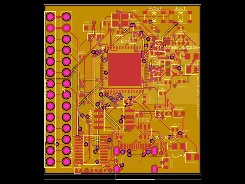 More from this authorseveibar/spi-display-webcam-interceptorThis collection of code defines various hardware components, including an crystal oscillator, microcontroller, voltage regulators, inductors, connectors, and logic gates, each represented with physical footprint, pin configurations, and 3D CAD models for PCB design and integration.
 Similar packageaura/diy-power-delivery-triggerThis hardware design implements a USB Type-C port with supporting power management and signal conditioning components, including a USB-C connector, a FUSB302 USB-C port controller, ESD protection diodes, a buck converter for 3.3V power regulation, an STM32 microcontroller for control and processing, an RGB LED indicator, push button, terminal block connections, and associated filtering and support components.
 Discover something newShiboSoftwareDev/mspm0g3507-usb-c-dev-boardThe circuit assembles a USB-C port with integrated ESD protection, power regulation, UART interface, and microcontroller (MSPM0G3507) with supporting components for USB data lines, CC termination, I2C, SPI, reset circuitry, and indicator LEDs.