seveibar/pedometer
This hardware setup integrates a Type-C connector, battery, display, and RF antenna connected through a microcontroller, USB interface, charging and fuel gauge ICs, along with associated passive components, enabling power management, data communication, and signal processing.
- Version
- 0.4.4
- License
- unset
- Stars
- 1
REGIONAL_ROUTING.md
# Spatial routing with stock Pipeline 9

The previous autoroutingphase schedule and all routingPhaseIndex assignments have been removed. The active board now uses one full-board `beta_pipeline9` pass with ordinary placement groups, explicit fanouts and selected source-defined traces. The earlier breakout boundary markers and their implicit routing passes have also been removed. No custom routing callbacks or router modifications are used.

The charger, MCU, sensor and fuel gauge were adjusted one region at a time. A single global pass routes all remaining connections, using the completed source-defined copper. Electrical nets and clearances are retained. C12 is rotated to put its supply pad toward the MCU; its existing ground-path anchor is adjusted for that rotation. R12 is moved near the clock exit, and C12 is shifted down to open the west-side signal corridor. The MCU exposed pad now has an explicit via path on inner1 to its ground pin, avoiding a fine-pitch surface escape.

A stock-core incompatibility was found while adding breakout groups: custom React schematic symbols delay component port initialization until after automatic breakout discovery. Proposed core patches were rejected by a duplicate-port regression check and removed. Four components now use the default schematic representation (`symbol={undefined}`), retaining their original PCB footprints and pin labels. The installed core is byte-identical to its original version.

## Active comparison

Trial 65 removed all breakout directives while retaining the explicit copper established through regional work. The active source has a single full-board routing pass. Trial 66 moves the JST clock via off its pad; trial 67 moves the pull-up supply vias and their bottom-layer link outside the resistor footprints. Trial 67 completed the full-board route with one raw RF trace-clearance error. Trial 72 resolves the last remaining error: the full board passes raw DRC with 138 traces and 115 vias.

## Trials

- No-region baseline: full board fails on WAKE_MR_N.
- Charger-only automatic boundary discovery: three direct traces found; named-net terminals remain outside the regional solve.
- Explicit charger port boundaries: 13 connections assigned to the region.
- Align charger boundaries to ball rows/columns: all 13 connections route.
- Repeat with unmodified core and default symbols: charger still passes.
- MCU region: all 25 boundary connections route.
- Sensor region: all nine boundary connections route.
- Add charger VIO boundary: charger now routes 14 connections.
- Fuel-gauge region: all nine pins route.
- Shared sensor supply exit: removes an external same-net loop.
- Sensor ground exit adjustment: resolves a fixed-copper conflict.
- Upgrade the published capacity autorouter from 0.0.866 to 0.0.880, retaining beta_pipeline9.
- Include both sensor bypass capacitors in the sensor region: 13 local connections route.
- Consolidate MCU VDDS exits inside its region: all local connections pass.
- Move the MCU I²C clock exit around the crystal area: global routing advances.
- Rotate the VDDD capacitor and correct its existing ground-path coordinates.
- Explicit charger IMAX exit removes a boundary collision with BAT1.
- Replace MCU EP surface breakout with a manual inner1 ground path: all four regions route and intermediate geometric checks pass; global routing fails on I2C_SCL between the pull-up and MCU exit.
- Move the clock exit west: rejected because the MCU regional path search stalls.

- Move the clock pull-up near the MCU exit: advances global routing; next failure is the VDDS2 surface loop.
- Connect VDDS2 to VDDS1 on inner2: intermediate geometry passes; next global failure is the crystal.
- Remove crystal boundary escapes and include the crystal in the MCU region: the stock tool still routes the internal crystal connections globally; the failure advances to the charger PMID branch.
- Give PMID1, PMID2 and VINLS a shared region exit: intermediate geometry passes; next global failure is display reset near C12.
- Move C12 down 1.3 mm and preserve its ground-path endpoint: passes high-density routing, then hits an internal SameNetViaMergerSolver exception on PMID.
- Upgrade stock capacity autorouter to 0.0.882: same via-merger exception, unchanged board.
- Move C3_VINLS beside the PMID exit: next failure is the clock branch at the gauge capacitor region.
- Move the gauge clock exit upward: next congestion is at the gauge SDA escape.
- Remove the old long manual SDA path: next failure is gauge BAT to its bypass capacitor.
- Move C7_GAUGE_BAT to the lower right of the gauge. The first position overlapped a courtyard and was rejected; the corrected position passes placement checks.
- Move C4_VSYS_SENSE left to open the charger escape area: next failure is the charger-to-gauge clock link.
- Use 0.10 mm clock traces, retaining all clearance limits: no change to the failure; confirmed 0.10 mm in the effective global input.
- Move the gauge clock exit to upper-left, facing the charger: advances to CHG_LP beneath C12.
- Remove C12's old manual ground path, preserving its previous 10 mm maximum length: advances to gauge battery-sense routing.
- Inspect the failed B01 routing cell. The BAT exit was only 0.18 mm below C8, while Pipeline 9 uses an internal 0.15 mm obstacle margin before accounting for trace width.
- Move the gauge BAT exit 0.5 mm down: advances to GAUGE_INT_N.
- Move the gauge interrupt pull-up above the gauge: next failure is clock to its pull-up.
- Move gauge clock exit north: next failure is VSYS.
- Restore trial 31 and remove only the VINLS manual path: rejected after a charger IMAX clearance error.
- Restore trial 31 and move C3 up 0.2 mm: next failure is ground routing.
- Contain the PMID network in the charger region, including C2 and C3 with explicit short paths: effective global input has no remaining PMID MST branches and intermediate geometry passes. Next failure is above the MCU.
- Connect VDDS3 to VDDS1 on inner2, with two distinct, spaced vias on the VDDS1 pad: geometry passes; next congestion is at gauge SDA.
- Remove the old manual SDA path on this branch: next failure is an immutable sensor VDDIO surface route.
- Connect sensor VDDIO to VDD on inner2: geometry passes; next failure is ACCEL_INT1.
- Move the sensor interrupt exit up: advances to the clock link.
- Combine the previously tested gauge layout with the newer charger/MCU/sensor routing: geometry passes; global high-density convergence fails.
- Inspect all external exits against Pipeline 9's internal obstacle margin: SDX and INT1 are too close to local ground traces despite passing physical board DRC.
- Move INT1 beyond the local ground straps to (13, -0.3): build in progress.

Full-board raw DRC, rather than regional completion, is the acceptance criterion. No error records are filtered and no generated copper is patched after routing.

### Later full-board work

- Trial 54 adds a physical SDA exit via; all boundary endpoints then pass the internal-margin comparison.
- Trial 55 replaces the sensor SDO ground loop with an inner1 connection.
- Trial 56 defines the charger ground return to C3 on bottom.
- Trial 57 defines the pull-up supply link on bottom.
- Trial 58 defines SWCLK to the JST connector on bottom, including the connector in the MCU placement group.
- Trial 59 removes the redundant MCU ground breakout so the manual EP/GND connection is recognized in the global connectivity input.
- Trials 60–61 define the wake-button route on inner1 and correct its clearance to the charger supply via.
- Trial 62 defines the display-power control route on bottom.
- Trial 63 defines the short gauge-interrupt route and includes R10/R12 in the gauge group.
- Trial 64 offsets the sensor VDD via within its pad; all regional geometry checks pass but global routing still fails.
- Trial 65 removes all virtual boundary markers and breakout passes. Global routing now runs once with the completed manual copper retained.
- Trial 66 moves the SWCLK connector via above its pad, clearing a ground-routing blockage.
- Trial 67 moves the R10/R12 supply vias and bottom wire outside their footprints: full board routed, 138 traces and 113 vias, one RF clearance error.

A review of stock core 0.0.1845 found no change relevant to the active routing failures; it was not installed. Core remains unmodified at 0.0.1837. The standalone SDA exit via was removed with the virtual boundary setup in trial 65.

- Trial 68 adds an inner1 RF ground return: rejected because global SWDIO routing fails.
- Trial 69 offsets the short RF signal path: rejected because global VSYS routing fails.
- Trial 70 retains trial 67 and narrows only the short MCU-to-C21 RF trace from 0.18 mm to 0.12 mm: full board routed with the RF clearance error resolved; one pad-to-trace clearance error remains at SW1. The initial 180 s timeout was insufficient; the same design completed with 600 s allowed.

- Trial 71 moves the SW1 pin2-to-pin1 source-defined strap to the left of the button footprint, away from its opposite contacts: no improvement; Pipeline 9 rewrites the preloaded surface strap to the same failing geometry.

- Trial 72 moves that strap to bottom with off-pad vias left of the footprint: full board routed with **zero raw DRC errors**, 138 traces and 115 vias. Cold-cache site build and validation passed.

## Crystal update, v0.4.2

The subsequent crystal-routing task reduces X48P from three vias to two and preserves zero vias on X48N, with original placement retained. The full-board 100× effort build passes raw DRC. See CRYSTAL_ROUTING.md and VALIDATION.md for current counts.

## Zero-via crystal update, v0.4.3

Y1 is rotated to 315° at (9, 0) mm. Both crystal signals now route on top with zero vias. Local ground-return changes and an RF-path bend preserve full-board routing with zero raw DRC errors. See CRYSTAL_ROUTING.md and VALIDATION.md for the current result.
Related Packages
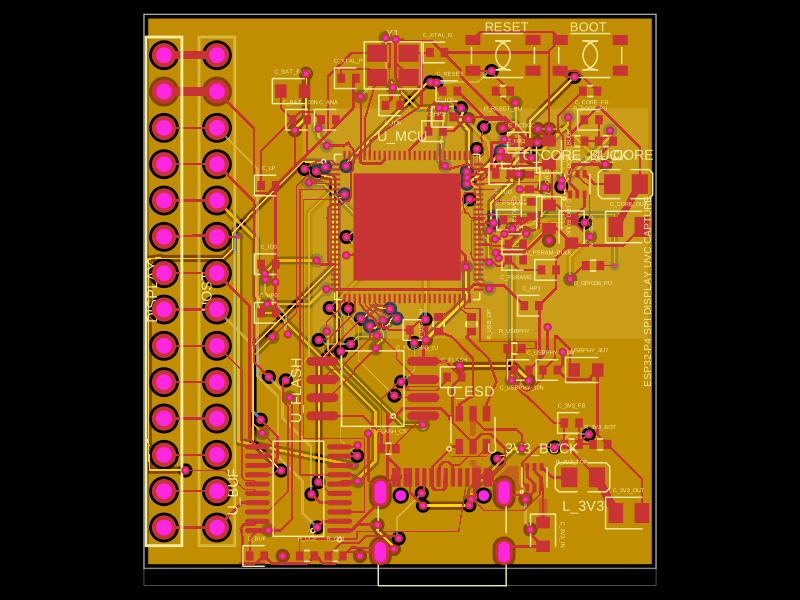 More from this authorseveibar/spi-display-webcam-interceptorThis collection of code defines various hardware components, including an crystal oscillator, microcontroller, voltage regulators, inductors, connectors, and logic gates, each represented with physical footprint, pin configurations, and 3D CAD models for PCB design and integration.
 Similar packageaura/diy-power-delivery-triggerThis hardware design implements a USB Type-C port with supporting power management and signal conditioning components, including a USB-C connector, a FUSB302 USB-C port controller, ESD protection diodes, a buck converter for 3.3V power regulation, an STM32 microcontroller for control and processing, an RGB LED indicator, push button, terminal block connections, and associated filtering and support components.
 Discover something newShiboSoftwareDev/mspm0g3507-usb-c-dev-boardThe circuit assembles a USB-C port with integrated ESD protection, power regulation, UART interface, and microcontroller (MSPM0G3507) with supporting components for USB data lines, CC termination, I2C, SPI, reset circuitry, and indicator LEDs.