seveibar/pedometer
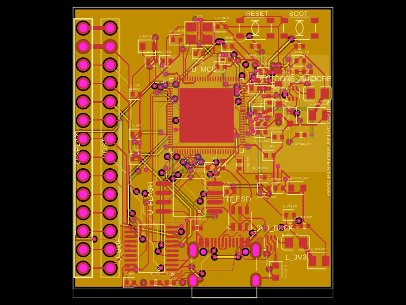
This hardware setup integrates a Type-C connector, battery, display, and RF antenna connected through a microcontroller, USB interface, charging and fuel gauge ICs, along with associated passive components, enabling power management, data communication, and signal processing.
- Version
- 0.4.4
- License
- unset
- Stars
- 1
DESIGN.md
> Current status: full-board stock Pipeline 9 routing passes raw DRC. See VALIDATION.md for evidence and remaining hardware-review warnings.

# Electrical design and firmware contract

## Power architecture

```text
USB-C 5 V ── BQ25150 IN
                 PMID ── VINLS → programmable LDO → SYS_VDD → CC2340R5 + BMA400
                                                          └→ P-MOS → DISP_VDD → OLED
Protected cell + ── BQ27427 BAT / internal shunt / SRX ── BQ25150 BAT
Protected cell − ── system ground
Cell NTC ── charger TS, with 10 kΩ parallel resistor
```

`VSYS` in the source is the gauge SRX / charger BAT node, not the regulated system rail. All cell charge and discharge current passes through the gauge. Do not connect the battery directly to PMID or SYS_VDD. BQ27427 VDD is its private regulator output, with only its bypass capacitor attached.

The MCU boots at the BQ25150 reset LDO voltage of 1.8 V. A firmware-controlled transition to 3.3 V supports the bench OLED. BQ25150 specifies VINLS ≥ VLDO + 0.5 V for LDO operation; allow margin and inhibit the display below 3.9 V battery voltage. At low battery, turn the display off, then return SYS_VDD to 1.8 V. Check supply transitions and actual headroom on hardware. Do not claim a 3.3 V rail over the entire LiPo discharge range.

BQ25150 VDD is always 1.8 V and is used only for its required capacitor. VIO follows SYS_VDD. `/LP` has an external 100 kΩ pull-down: low is the idle state. There is no continuous pull-up current while idle. Raise `/LP` before charger I²C operations on battery and allow the documented wake time. CE is left open, using the device's internal enable pull-down. ADCIN and INT are intentionally unconnected.

The reset charge current is 10 mA; reset input limit is 100 mA. Keep those conservative settings for initial bring-up. The inherited 10 kΩ IMAX resistor is **not a 10 mA hardware charge limit**. Never increase the register current without checking the selected cell's data sheet. R5 is an unpopulated bench thermistor bypass, not a production option. The cell must include protection; this PCB does not add a separate cell protection IC.

## MCU signal map (24-pin RGE package)

| Pad | GPIO/function | Board signal |
|---:|---|---|
| 3 | DIO8 | I2C_SDA |
| 19 | DIO6 | I2C_SCL |
| 5 | DIO12 | ACCEL_INT1 |
| 12 | DIO24 | DISP_SCLK |
| 6 | DIO13 | DISP_MOSI |
| 4 | DIO11 | DISP_CS |
| 10 | DIO21 | DISP_DC |
| 15 | DIO4 | DISP_RST |
| 9 | DIO20 | DISP_PWR_N |
| 14 | DIO3 | CHG_LP |
| 7 | DIO16 | SWDIO |
| 8 | DIO17 | SWDCK |
| 13 | RSTN | RESET_N |

The SPI and I²C pin choices follow the RGE LaunchPad reference assignments. Confirm them in the selected TI SDK SysConfig before compiling. BMA400 INT2 and gauge GPOUT are not connected to the MCU; poll battery status infrequently. R10, the gauge interrupt pull-up, is unpopulated.

## I²C / SPI cross-reference

| Device | Wired interface | Address / signals | Alternate interface |
|---|---|---|---|
| BQ25150 | I²C | 7-bit 0x6B | none |
| BQ27427 | I²C | 7-bit 0x55 | none |
| BMA400 | I²C | 7-bit 0x14; CSB high, SDO low | SPI: SCX=SCLK, SDX=MOSI, SDO=MISO, CSB=CS; requires board rewiring |
| OLED / Adafruit 661 | dedicated four-wire SPI | SCLK, MOSI, CS, DC, RESET | Other SSD1306 modules can offer I²C 0x3C/0x3D, but this PCB has no OLED I²C pull-ups and that is not a drop-in option |

Use I²C at 100 kHz initially. The 10 kΩ pull-ups allow about 118 pF for a 1 µs rise time, but only about 35 pF for the 300 ns fast-mode limit (`tr ≈ 0.8473 × R × C`). Measure rise time before using 400 kHz. Do not rely on duplicate pull-ups from an external module.

## Connectors

J2 is JST-SH 3-pin, BM03B-SRSS-TB: **1 = BAT_CELL+, 2 = NTC, 3 = GND**. NTC is 10 kΩ at 25 °C to battery negative; its beta and thermal attachment must match the charging thresholds. Many retail LiPos have different connectors/polarity and no NTC. Build and continuity-test the harness.

J3 is JST-SH 7-pin, BM07B-SRSS-TB:

| Pin | PCB signal | Connect to OLED |
|---:|---|---|
| 1 | DISP_VDD | Vin / 3.3 V module supply |
| 2 | GND | GND |
| 3 | DISP_SCLK | CLK |
| 4 | DISP_MOSI | DATA |
| 5 | DISP_CS | CS |
| 6 | DISP_DC | D/C |
| 7 | DISP_RST | RESET |

This is a **custom cable pinout**, not the physical pin order of an Adafruit header. No extra raw-panel charge-pump capacitors are on the main PCB: the selected display must be a complete powered module. Adafruit 661 lists about 20 mA typical display current and a 3.3 V supply requirement.

Programming connector J4 is a five-pin, 1.0 mm-pitch JST-SH BM05B-SRSS-TB(LF)(SN), top entry. Mating housing: SHR-05V-S; use compatible SH contacts or a precrimped SH harness. This is a custom SWD pinout, not a standard debug cable or Qwiic/STEMMA QT pinout.

| J4 circuit number | Signal | Debugger connection |
|---|---|---|
| 1 | SWDIO | SWD data |
| 2 | SWDCK | SWCLK |
| 3 | RESET_N | Active-low reset |
| 4 | GND | Ground |
| 5 | SYS_VDD / VTREF | Target-voltage sense |

Pin 1 is marked by the imported footprint dot. With the board viewed from above and USB at lower left, pin 1 is the rightmost J4 signal pad. Follow the housing's circuit numbering when making the cable; do not infer numbering from wire colors. Both mechanical solder tabs are electrically unconnected.

The debugger must sense/follow the target rail, including the 1.8 V boot state and possible 3.3 V display state. J4 pin 5 is a voltage-reference output, not an unregulated external power input. Power the target from USB or its battery and disable probe power injection. Keep the debug cable short; begin at 100 kHz SWD for bring-up. TP6 remains as a charger power-good measurement pad.

Connector reference: [JST SH series drawing](https://www.jst-mfg.com/product/pdf/eng/eSH.pdf).

## Firmware implementation sequence

1. Start from TI's CC2340R5 BLE peripheral example for the exact RGE device. Select the internal LF RC clock with the silicon/SDK CLK_01 workaround. DIO3/DIO4 are used as GPIO, so no external 32 kHz crystal can be fitted on this revision. Synchronize calendar time from the phone.
2. Before enabling peripherals, set display SCLK/MOSI/CS/DC/RESET low with internal pulls disabled; hold DISP_PWR_N high. These five signals must all remain low whenever the OLED is unpowered. Otherwise GPIO protection structures can back-power the OLED even though its supply is switched.
3. Raise CHG_LP; wait for charger wake. Probe the management bus. Confirm BMA400 chip identity and PMIC identities before writes.
4. Configure charge voltage, charge/termination currents, NTC thresholds and gauge design capacity/chemistry for the exact cell. Retain the 10 mA reset charge setting until cell limits are established. Clear/read charger flags according to its data sheet; do not blindly rewrite reserved bits.
5. Configure BMA400 normal-mode hardware step counting and INT1 activity/tap interrupt with Bosch's SensorAPI. Use the hardware counter; do not wake the MCU for every accelerometer sample. Keep a software accumulator across counter rollover/reset and checkpoint infrequently to avoid flash wear.
6. When voltage permits, write LDOCTRL at 0x1D to 0xEC for 3.3 V (enabled, LDO mode), wait for settling, and recheck bus operation. Reset value 0xB0 is 1.8 V. Never select load-switch mode, which would expose logic to PMID.
7. For display wake: keep reset and signal lines low, enable power, wait for module start-up, initialize SSD1306, then display step count/battery. After about 5 seconds send display-off; set every display signal low; switch off the MOSFET. Do not leave CS high on an unpowered module.
8. Return CHG_LP low after queries. Use 1–2 second advertising intervals as a starting point and long peripheral connection intervals/latency where the phone permits. Measure total current rather than assuming the theoretical BLE duty cycle.
9. Provide the standard BLE Battery Service and a custom step-count characteristic with read/notify, plus a time/configuration write characteristic. Use authenticated pairing for configuration writes. Persist steps across ordinary resets and clearly indicate a fresh counter after a factory reset.
10. Below the display cutoff, disable the OLED and return LDOCTRL to 0xB0. Continue counting/syncing until the verified cell/system cutoff. For shipping, put the gauge into its documented shutdown state as well as commanding PMIC ship mode; the gauge is upstream of the PMIC and otherwise keeps consuming current.

This is a firmware contract and bring-up sequence; a flashable application and phone application are not included or hardware-tested.

## RF / physical implementation

The filter is 1.5 pF shunt / 2.8 nH series / 1.5 pF shunt, followed by a 15 pF DC block. Short top-layer routes are explicit in TSX. Match the inductor's RF impedance/Q, not just its nominal inductance. The 0.12 mm MCU-to-C21 segment and 0.18 mm remaining RF trace widths are provisional: ask the fabricator to solve a 50 Ω feed against the actual dielectric/copper stack-up. A DRC pass does not validate impedance or harmonic suppression.

Four layers, 1.0 mm nominal FR-4. Inner1, top and bottom have GND pours; routing can also occupy inner layers, so inspect the returned copper for uninterrupted return paths under the RF filter. Antenna inner/bottom keepouts and the top-pour notch are in the source. Keep the battery, OLED metal, enclosure metal and cables away from the antenna volume. Johanson's reference ground geometry and enclosure tuning still need a physical RF review.

The BQ25150 uses 0.4 mm-pitch DSBGA with 0.2 mm lands, 0.10/0.20 mm via geometry and 0.05 mm pad/trace clearance. This is HDI assembly work, not a beginner hand-solderable board. Agree via type, filling/capping, layer spans and stack-up with the fabricator before export approval. Revision D enables blind/buried vias explicitly and uses source-defined fanouts to inner1 ground and inner2 SYS_VDD pours. Full-board routing passes raw DRC, but no fabrication via map is approved. See VALIDATION.md. The model is not a qualified HDI stack-up.

## Primary references

- [TI CC2340R5 data sheet](https://www.ti.com/lit/ds/symlink/cc2340r5.pdf)
- [TI RGE reference schematic, revision E6](https://e2e.ti.com/cfs-file/__key/communityserver-discussions-components-files/538/lp_2D00_em_2D00_cc2340r5_2D00_rge_5F00_Schematic.pdf)
- [TI hardware design guide SWRA834A](https://www.ti.com/lit/an/swra834a/swra834a.pdf)
- [TI BQ25150 data sheet](https://www.ti.com/lit/ds/symlink/bq25150.pdf)
- [TI BQ27427 data sheet](https://www.ti.com/lit/ds/symlink/bq27427.pdf)
- [TI gauge supported capacity](https://www.ti.com/product/BQ27427)
- [Bosch BMA400 data sheet](https://www.bosch-sensortec.com/media/boschsensortec/downloads/datasheets/bst-bma400-ds000.pdf)
- [Bosch BMA400 product and step-counter consumption](https://www.bosch-sensortec.com/en/products/motion-sensors/accelerometers/bma400)
- [Adafruit 661 display specification](https://www.adafruit.com/product/661)

Antenna reference: [Johanson terminal and mounting guide](https://www.johansontechnology.com/docs/3828/Antenna-2450AT18A0100002E-Rev2.0.pdf). This is an AEC successor-family document; verify the exact legacy ordering code. Pin 2 is mechanically soldered but electrically NC. The current PCB antenna position is along the edge, while the reference recommends a corner and a separate tuning network. Resolve placement/ground geometry and provision the final matching network before the RF prototype release.

No fabrication drill map is released pending fabricator approval of the HDI stackup and via spans.
Related Packages
 More from this authorseveibar/spi-display-webcam-interceptorThis collection of code defines various hardware components, including an crystal oscillator, microcontroller, voltage regulators, inductors, connectors, and logic gates, each represented with physical footprint, pin configurations, and 3D CAD models for PCB design and integration.
 Similar packageaura/diy-power-delivery-triggerThis hardware design implements a USB Type-C port with supporting power management and signal conditioning components, including a USB-C connector, a FUSB302 USB-C port controller, ESD protection diodes, a buck converter for 3.3V power regulation, an STM32 microcontroller for control and processing, an RGB LED indicator, push button, terminal block connections, and associated filtering and support components.
 Discover something newShiboSoftwareDev/mspm0g3507-usb-c-dev-boardThe circuit assembles a USB-C port with integrated ESD protection, power regulation, UART interface, and microcontroller (MSPM0G3507) with supporting components for USB data lines, CC termination, I2C, SPI, reset circuitry, and indicator LEDs.