seveibar/nema17-stepper-motor-driver-tmc2209-usb-pd
RP2040-based USB-C PD stepper-motor controller with TMC2209 drive, AS5600 position feedback, TMP102 thermal shutdown, current/voltage telemetry, RGB status LED, and protected buzzer alarm circuitry.
- Version
- 0.2.0
- License
- unset
- Stars
- 0
schematic/TelemetrySection.tsx
import { TZ_0807Z1RGB_5V_I4_MS_5mA_ } from "../imports/TZ_0807Z1RGB_5V_I4_MS_5mA_";
import { SN74AHCT1G125DBVR } from "../imports/SN74AHCT1G125DBVR";
import { INA180A1IDBVR } from "../imports/INA180A1IDBVR";
import { BSS84 } from "../imports/BSS84";
import { AO3400A } from "../imports/AO3400A";
const rgb = {schSheetName:"telemetry", schSectionName:"rgb"};
const voltage = {schSheetName:"telemetry", schSectionName:"voltage"};
const current = {schSheetName:"telemetry", schSectionName:"current"};

/** PD voltage and positive motor-supply current are separate measurements.
 * The TMC2209 phase-current shunts stay dedicated to its chopper control.
 */
export const TelemetrySection = () => <>
  <schematicsheet name="telemetry" displayName="RGB Status & Power Telemetry" sheetIndex={7} sheetWidth="310mm" sheetHeight="400mm">
    <schematicsection name="rgb" />
    <schematicsection name="voltage" />
    <schematicsection name="current" />
    <schematictext text="Dim Addressable RGB — GPIO25" schX={-6} schY={15} fontSize={0.3} />
    <schematictext text="Motor Supply Current — ADC3, 1 V/A" schX={-6} schY={4} fontSize={0.3} />
    <schematictext text="Switched PD Voltage Divider — ADC2, ratio 11" schX={-6} schY={-6} fontSize={0.3} />
  </schematicsheet>
  <TZ_0807Z1RGB_5V_I4_MS_5mA_ name="D_RGB" schWidth={1.8} schHeight={1.5} schPinArrangement={{leftSide:{pins:[3],direction:"top-to-bottom"},rightSide:{pins:[1],direction:"top-to-bottom"},topSide:{pins:[4],direction:"left-to-right"},bottomSide:{pins:[2],direction:"left-to-right"}}} pcbX={-6.0} pcbY={3.5} schX={6} schY={10.0} noConnect={["DOU"]} {...rgb}/>
  <SN74AHCT1G125DBVR name="U_RGB_BUFFER" schWidth={1.8} schHeight={1.5} schPinArrangement={{leftSide:{pins:[2,1],direction:"top-to-bottom"},rightSide:{pins:[4],direction:"top-to-bottom"},topSide:{pins:[5],direction:"left-to-right"},bottomSide:{pins:[3],direction:"left-to-right"}}} layer="bottom" pcbX={-5.0} pcbY={-9.0} schX={0} schY={10.0} {...rgb}/>
  {[
    ["R_RGB_DATA","100","C25076",-1.5,-9.0,3,0],
    ["R_RGB_PD","100k","C25741",-10.5,-12.0,-3,-2],
  ].map(([name,value,part,x,y,sx,sy])=><resistor key={name} name={name as string} resistance={value as string} footprint="0402" layer="bottom"
    supplierPartNumbers={{jlcpcb:[part as string]}} pcbX={x as number} pcbY={y as number} schX={sx as number} schY={(sy as number) + (10)} {...rgb}/>)}
  <capacitor name="C_RGB" capacitance="100nF" footprint="0402" supplierPartNumbers={{jlcpcb:["C1525"]}}
    pcbX={-3.5} pcbY={5.5} pcbRotation={90} schX={9} schY={10.0} schOrientation="vertical" maxDecouplingTraceLength={6} {...rgb}/>
  <capacitor name="C_RGB_BUFFER" capacitance="100nF" footprint="0402" supplierPartNumbers={{jlcpcb:["C1525"]}}
    layer="bottom" pcbX={-5.0} pcbY={-12.0} schX={-3} schY={13.0} schOrientation="vertical" maxDecouplingTraceLength={4} {...rgb}/>

  <resistor name="R_BUS_SHUNT" resistance="0.05" tolerance="1%" footprint="1206" supplierPartNumbers={{jlcpcb:["C912768"]}}
    manufacturerPartNumber="RLM12FTCMR050" layer="bottom" pcbX={3.5} pcbY={7.0} schX={0} schY={0.0} {...current}/>
  <INA180A1IDBVR name="U_BUS_CURRENT" schWidth={1.8} schHeight={1.5} schPinArrangement={{leftSide:{pins:[3,4],direction:"top-to-bottom"},rightSide:{pins:[1],direction:"top-to-bottom"},topSide:{pins:[5],direction:"left-to-right"},bottomSide:{pins:[2],direction:"left-to-right"}}} layer="bottom" pcbX={4.0} pcbY={11.0} schX={0} schY={-3.0} {...current}/>
  <capacitor name="C_BUS_CURRENT" capacitance="100nF" footprint="0402" supplierPartNumbers={{jlcpcb:["C1525"]}}
    layer="bottom" pcbX={7.5} pcbY={12.0} schX={-3} schY={-3.0} schOrientation="vertical" maxDecouplingTraceLength={4} {...current}/>
  <resistor name="R_CURRENT_FILTER" resistance="1k" footprint="0402" supplierPartNumbers={{jlcpcb:["C11702"]}}
    layer="bottom" pcbX={0.0} pcbY={12.0} schX={3} schY={-3.0} {...current}/>
  <capacitor name="C_CURRENT_FILTER" capacitance="100nF" footprint="0402" supplierPartNumbers={{jlcpcb:["C1525"]}}
    layer="bottom" pcbX={0.5} pcbY={15.0} schX={6} schY={-3.0} schOrientation="vertical" {...current}/>

  {/* Disconnect the voltage divider when logic power is absent: the two USB
      connectors may be plugged independently. R_GATE limits PMOS |Vgs|. */}
  <BSS84 name="Q_VSENSE" schWidth={1.8} schHeight={1.5} schPinArrangement={{leftSide:{pins:[2],direction:"top-to-bottom"},rightSide:{pins:[3],direction:"top-to-bottom"},bottomSide:{pins:[1],direction:"left-to-right"}}} layer="bottom" pcbX={11.0} pcbY={7.5} schX={-3} schY={-9.0} {...voltage}/>
  <AO3400A name="Q_VSENSE_ENABLE" layer="bottom" pcbX={10.5} pcbY={11.5} schX={-3} schY={-14.0} {...voltage}/>
  {[
    ["R_VSENSE_PU","100k","C25741",14.5,8.0,0,2],
    ["R_VSENSE_GATE","100k","C25741",14.0,10.5,-3,-2.5],
    ["R_VSENSE_TOP","100k","C25741",7.5,10.0,0,0],
    ["R_VSENSE_BOTTOM","10k","C25744",7.0,8.5,3,-2],
  ].map(([name,value,part,x,y,sx,sy])=><resistor key={name} name={name as string} resistance={value as string} tolerance="1%" footprint="0402" layer="bottom"
    supplierPartNumbers={{jlcpcb:[part as string]}} pcbX={x as number} pcbY={y as number} schX={sx as number} schY={(sy as number) + (-9)} {...voltage}/>)}
  <capacitor name="C_VSENSE" capacitance="100nF" footprint="0402" supplierPartNumbers={{jlcpcb:["C1525"]}}
    layer="bottom" pcbX={0.5} pcbY={10.0} schX={6} schY={-11.0} schOrientation="vertical" {...voltage}/>
  {[
    ["RGB_GPIO",".MCU > .U1 > .GPIO25",".U_RGB_BUFFER > .A"],
    ["RGB_PULLDOWN",".U_RGB_BUFFER > .A",".R_RGB_PD > .pin1"],
    ["RGB_PD_GND",".R_RGB_PD > .pin2","net.GND"],
    ["RGB_BUFFER_ENABLE",".U_RGB_BUFFER > .N_OE","net.GND"],
    ["RGB_BUFFER_GND",".U_RGB_BUFFER > .GND","net.GND"],
    ["RGB_DATA_R",".U_RGB_BUFFER > .Y",".R_RGB_DATA > .pin1"],
    ["RGB_DIN",".R_RGB_DATA > .pin2",".D_RGB > .DIN"],
    // Use the programming USB's 5 V, never the negotiated motor VBUS.
    ["RGB_5V",".MCU > .J_USB > .A4B9",".U_RGB_BUFFER > .VCC"],
    ["RGB_VDD",".U_RGB_BUFFER > .VCC",".D_RGB > .VDD"],
    ["RGB_GND",".D_RGB > .GND","net.GND"],
    ["RGB_CAP",".D_RGB > .VDD",".C_RGB > .pin1"],
    ["RGB_CAP_GND",".C_RGB > .pin2","net.GND"],
    ["RGB_BUFFER_CAP",".U_RGB_BUFFER > .VCC",".C_RGB_BUFFER > .pin1"],
    ["RGB_BUFFER_CAP_GND",".C_RGB_BUFFER > .pin2","net.GND"],
    ["BUS_SHUNT_FEED",".F_MOTOR_VBUS > .pin2",".R_BUS_SHUNT > .pin1"],
    ["BUS_CURRENT_POS",".R_BUS_SHUNT > .pin1",".U_BUS_CURRENT > .IN_POS"],
    ["BUS_CURRENT_NEG",".R_BUS_SHUNT > .pin2",".U_BUS_CURRENT > .IN_NEG"],
    ["BUS_CURRENT_3V3",".MCU > .L_AVDD > .pin1",".U_BUS_CURRENT > .VS"],
    ["BUS_CURRENT_GND",".U_BUS_CURRENT > .GND","net.GND"],
    ["BUS_CURRENT_BYPASS",".U_BUS_CURRENT > .VS",".C_BUS_CURRENT > .pin1"],
    ["BUS_CURRENT_BYPASS_GND",".C_BUS_CURRENT > .pin2","net.GND"],
    ["CURRENT_FILTER",".U_BUS_CURRENT > .OUT",".R_CURRENT_FILTER > .pin1"],
    ["CURRENT_FILTER_C",".R_CURRENT_FILTER > .pin2",".C_CURRENT_FILTER > .pin1"],
    ["CURRENT_FILTER_GND",".C_CURRENT_FILTER > .pin2","net.GND"],
    ["CURRENT_ADC3",".R_CURRENT_FILTER > .pin2",".MCU > .U1 > .GPIO29_ADC3"],
    ["VOLTAGE_PD_INPUT",".J_MOTOR_USB > .A4B9",".Q_VSENSE > .source"],
    ["VSENSE_PU_SOURCE",".Q_VSENSE > .source",".R_VSENSE_PU > .pin1"],
    ["VSENSE_PU_GATE",".Q_VSENSE > .gate",".R_VSENSE_PU > .pin2"],
    ["VSENSE_GATE_R",".Q_VSENSE > .gate",".R_VSENSE_GATE > .pin1"],
    ["VSENSE_GATE_SINK",".R_VSENSE_GATE > .pin2",".Q_VSENSE_ENABLE > .D"],
    ["VSENSE_ENABLE",".Q_VSENSE_ENABLE > .G",".MCU > .L_AVDD > .pin1"],
    ["VSENSE_ENABLE_GND",".Q_VSENSE_ENABLE > .S","net.GND"],
    ["VSENSE_DIVIDER_TOP",".Q_VSENSE > .drain",".R_VSENSE_TOP > .pin1"],
    ["VSENSE_DIVIDER_JOIN",".R_VSENSE_TOP > .pin2",".R_VSENSE_BOTTOM > .pin1"],
    ["VSENSE_DIVIDER_GND",".R_VSENSE_BOTTOM > .pin2","net.GND"],
    ["VSENSE_FILTER",".R_VSENSE_BOTTOM > .pin1",".C_VSENSE > .pin1"],
    ["VSENSE_FILTER_GND",".C_VSENSE > .pin2","net.GND"],
    ["VOLTAGE_ADC2",".R_VSENSE_BOTTOM > .pin1",".MCU > .U1 > .GPIO28_ADC2"],
  ].map(([name,from,to])=><trace key={name} name={name} from={from} to={to} thickness={name==="BUS_SHUNT_FEED"?"0.5mm":"0.15mm"}/>)}
</>;
Related Packages
 More from this authorseveibar/1206_x4This code defines a PCB footprint for an 8-pin 1206-sized resistor network with surface-mount pads arranged on both sides in a compact rectangular package.
 Similar packageimrishabh18/rp2040-motor-controllerAn RP2040-based NEMA17 stepper-motor controller with USB-C programming and PD motor-power negotiation, DRV8825 dual H-bridge drive, current/temperature telemetry, protected power filtering, status RGB LED, buzzer alarm, and optional magnetic encoder.
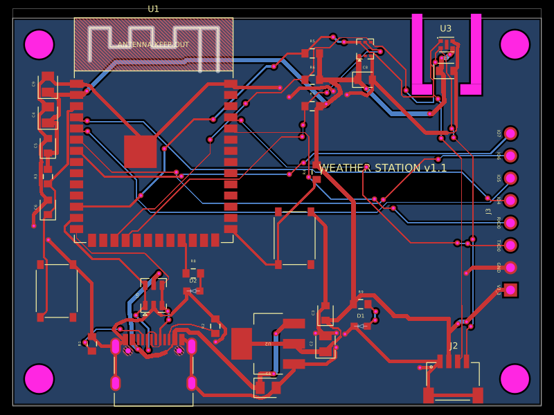 Discover something newolivergrabinski/tscircuit-weatherA 60×44 mm ESP32-S3 Wi‑Fi/BLE weather-station PCB with USB‑C power, 3.3 V regulation and ESD protection, temperature/humidity and UV/light sensors, status LEDs, buttons, Qwiic I²C expansion, debug GPIO header, and a printable enclosure.