seveibar/minimal-rp2040
This design features a Raspberry Pi RP2040 microcontroller with integrated decoupling capacitors, QSPI flash memory, crystal oscillator, and USB power circuitry, all mounted on a 65mm by 60mm four-layer PCB.
Usage: To import and use the RP2040 component in a tscircuit project: 1. Import the component: ```tsx import { RP2040 } from "@tsci/seveibar.minimal-rp2040" ``` 2. Use the component in a board: ```tsx <board> <RP2040 name="U3" pcbX={0} pcbY={0} connections={{ IOVDD1: "net.V3V3", // Add other required connections }} /> </board> ``` Key points: - Specify a name for the component - Set position using `pcbX` and `pcbY` - Define necessary network connections in the `connections` prop - Ensure proper power and ground connections
- Version
- 1.0.1
- License
- unset
- Stars
- 1
lib/thirdparty/RP2040Zero.tsx
// Rp2040Zero.tsx

type RP2040ZeroConnections = Partial<{
  V5: string
  GND: string
  V3_3: string
  GP29: string
  GP28: string
  GP27: string
  GP26: string
  GP15: string
  GP14: string

  GP0: string
  GP1: string
  GP2: string
  GP3: string
  GP4: string
  GP5: string
  GP6: string
  GP7: string
  GP8: string

  GP13: string
  GP12: string
  GP11: string
  GP10: string
  GP9: string
}>

export type Rp2040ZeroProps = {
  name: string
  pcbX?: number | string
  pcbY?: number | string
  pcbRotation?: number | string

  /**
   * Maps exposed RP2040-Zero pin labels (GND/3V3/GP0/...) to nets or ports,
   * e.g. { GND: "net.GND", "3V3": "net.VCC", GP0: "net.SDA", GP1: "net.SCL" }
   */
  connections?: RP2040ZeroConnections

  /**
   * Cutout size on the *carrier PCB* underneath the module.
   * Tune these if you want more/less clearance.
   */
  cutoutWidth?: number | string
  cutoutHeight?: number | string

  /**
   * If you ever want to disable the cutout.
   */
  includeCutout?: boolean
}

export const Rp2040Zero = ({
  name,
  pcbX,
  pcbY,
  pcbRotation,
  connections,
  includeCutout = true,
}: Rp2040ZeroProps) => {
  // Mechanical basics (mm) from Waveshare drawing:
  // Board: 18.0mm wide x 23.5mm tall
  // Castellated pitch: 2.54mm
  // Side pad centerlines: 1.38mm from each side edge => x = ±7.62mm
  // Side pad y positions: ±10.16mm down in 2.54mm steps
  const P = 2.54
  const X_SIDE = 3.5 * P // 7.62
  const Y_TOP = 4 * P // 10.16

  const leftLabels = [
    "V5",
    "GND",
    "V3_3",
    "GP29",
    "GP28",
    "GP27",
    "GP26",
    "GP15",
    "GP14",
  ] as const
  const rightLabels = [
    "GP0",
    "GP1",
    "GP2",
    "GP3",
    "GP4",
    "GP5",
    "GP6",
    "GP7",
    "GP8",
  ] as const
  const bottomLabels = ["GP13", "GP12", "GP11", "GP10", "GP9"] as const

  // Pin numbering convention used here:
  //  1..9   = left side top->bottom
  //  10..18 = right side top->bottom
  //  19..23 = bottom row left->right
  const pinLabels: Record<string, string> = {}
  leftLabels.forEach((lbl, i) => (pinLabels[`pin${1 + i}`] = lbl))
  rightLabels.forEach((lbl, i) => (pinLabels[`pin${10 + i}`] = lbl))
  bottomLabels.forEach((lbl, i) => (pinLabels[`pin${19 + i}`] = lbl))

  return (
    <group pcbX={pcbX} pcbY={pcbY} pcbRotation={pcbRotation}>
      {/* This chip is the "module footprint" that solders to the castellated edges */}
      <chip
        name={name}
        pinLabels={pinLabels}
        connections={connections}
        footprint={
          <footprint>
            {/* Side pads: longer inward (X direction) */}
            {leftLabels.map((_, i) => {
              const pin = String(1 + i)
              const y = Y_TOP - i * P + 0.3
              return (
                <smtpad
                  key={`L${pin}`}
                  portHints={[pin]}
                  pcbX={-X_SIDE}
                  pcbY={y}
                  width="2.0mm"
                  height="1.6mm"
                  shape="rect"
                />
              )
            })}

            {rightLabels.map((_, i) => {
              const pin = String(10 + i)
              const y = Y_TOP - i * P + 0.3
              return (
                <smtpad
                  key={`R${pin}`}
                  portHints={[pin]}
                  pcbX={+X_SIDE}
                  pcbY={y}
                  width="2.0mm"
                  height="1.6mm"
                  shape="rect"
                />
              )
            })}

            {/* Bottom pads: longer inward (Y direction) */}
            {bottomLabels.map((_, i) => {
              const pin = String(19 + i)
              const x = (-2 + i) * P // -5.08, -2.54, 0, +2.54, +5.08
              const y = -Y_TOP - 2 // -10.16
              return (
                <smtpad
                  key={`B${pin}`}
                  portHints={[pin]}
                  pcbX={x}
                  pcbY={y}
                  width="1.6mm"
                  height="2.0mm"
                  shape="rect"
                />
              )
            })}
          </footprint>
        }
      />

      {/* Carrier-board cutout: lets the *bottom-side* components of the RP2040-Zero
          drop into the hole so the module can sit flush (castellated-solder style). */}
      {includeCutout && (
        <cutout shape="rect" width={15.5} height={24} pcbX={0} pcbY={1} />
      )}
    </group>
  )
}
Related Packages
 More from this authortscircuit/autorouting-dataset-01This code manages the hardware and electronic components for circuit design and PCB layout, defining components like resistors, capacitors, transistors, connectors, and footprints, and providing tools for component placement, PCB topology, and electrical connections.
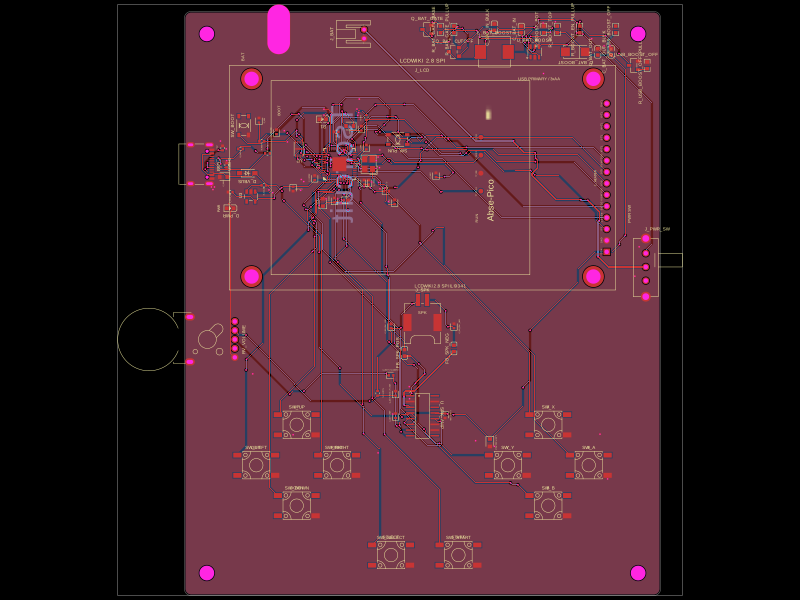 Similar packageabse/gameboyThis code defines the hardware mapping and schematic connections for a Raspberry Pi Pico-based development board featuring RP2040 microcontroller, USB-C connector, various power regulation components, decoupling capacitors, resistors, LEDs, headers, and supporting passive components for signal integrity and debugging.
 Discover something newimrishabh18/fitness_watchThis circuit integrates an ESP-12E microcontroller with various sensors, relays, and power management components, including an AO3400A transistor for switching loads, to enable wireless control and sensing functions.