seveibar/minimal-rp2040
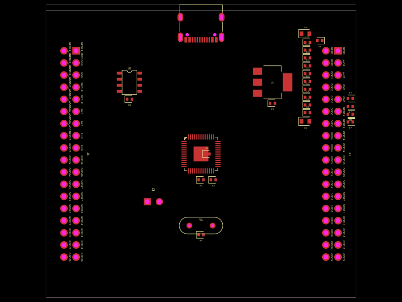
This design features a Raspberry Pi RP2040 microcontroller with integrated decoupling capacitors, QSPI flash memory, crystal oscillator, and USB power circuitry, all mounted on a 65mm by 60mm four-layer PCB.
Usage: To import and use the RP2040 component in a tscircuit project: 1. Import the component: ```tsx import { RP2040 } from "@tsci/seveibar.minimal-rp2040" ``` 2. Use the component in a board: ```tsx <board> <RP2040 name="U3" pcbX={0} pcbY={0} connections={{ IOVDD1: "net.V3V3", // Add other required connections }} /> </board> ``` Key points: - Specify a name for the component - Set position using `pcbX` and `pcbY` - Define necessary network connections in the `connections` prop - Ensure proper power and ground connections
- Version
- 1.0.1
- License
- unset
- Stars
- 1
RP2040_CONNECTIONS.md
PCB
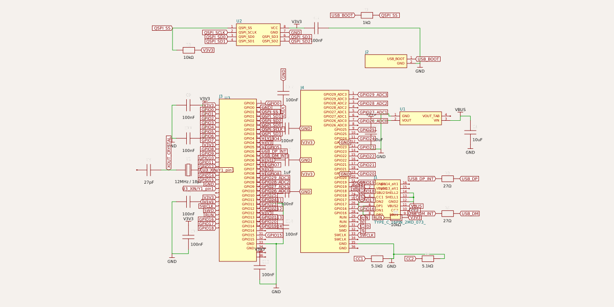
Schematic
# RP2040 Minimal Design Example – Circuit Documentation

This document describes the official **RP2040 Minimal Design Example** from Raspberry Pi’s _Hardware design with RP2040_ guide. It explains the **major ICs** and how every functional block is wired: power, internal 1.1 V rail, flash, crystal, USB, I/O headers, and debug. :contentReference[oaicite:0]{index=0}

---

## 1. Major components

| Ref      | Part                               | Function                                                                                                        |
| -------- | ---------------------------------- | --------------------------------------------------------------------------------------------------------------- |
| U3       | **RP2040** (QFN‑56)                | Main MCU: dual‑core Cortex‑M0+, 3.3 V I/O, internal 1.1 V core regulator. :contentReference[oaicite:1]{index=1} |
| U1       | **NCP1117‑3.3** LDO regulator      | Converts USB 5 V (VBUS) to 3.3 V for RP2040 and peripherals. :contentReference[oaicite:2]{index=2}              |
| U2       | **W25Q128JVS** (16 MiB QSPI flash) | External code/data storage on RP2040’s QSPI bus. :contentReference[oaicite:3]{index=3}                          |
| Y1       | **ABLS‑12.000MHZ‑B4‑T** crystal    | 12 MHz reference clock for RP2040 PLLs & USB. :contentReference[oaicite:4]{index=4}                             |
| J1       | Micro‑USB B socket                 | 5 V power input and USB D+/D− data. :contentReference[oaicite:5]{index=5}                                       |
| J2       | 2‑pin “USB_BOOT” header            | Forces BOOTSEL mode via QSPI_SS strap. :contentReference[oaicite:6]{index=6}                                    |
| J3, J4   | Two 2×18 2.54 mm headers           | Bring out GPIO0–GPIO29 plus many grounds. :contentReference[oaicite:7]{index=7}                                 |
| (C*, R*) | Capacitors & resistors             | Decoupling, crystal load, USB series resistors, boot strap, etc. :contentReference[oaicite:8]{index=8}          |

---

## 2. Power system

### 2.1 Input from USB

- **Source:**
  - J1.VBUS (5 V from USB host) is the only power input in the minimal design. :contentReference[oaicite:9]{index=9}
- **Protection / regulation:**
  - VBUS → **U1 (NCP1117‑3.3)** input pin.
  - **C1 (10 µF)** from VBUS to GND close to U1 (LDO input capacitor).
  - **C4 (10 µF)** from 3V3 output to GND close to U1 (LDO output capacitor). :contentReference[oaicite:10]{index=10}
- **3V3 net:**
  - U1 output creates main **+3V3** rail.
  - +3V3 feeds:
    - All RP2040 **IOVDD** pins.
    - **USB_VDD** (USB PHY supply).
    - **ADC_AVDD** (ADC analog supply).
    - VCC of flash U2.
    - Pull‑ups and other 3.3 V logic. :contentReference[oaicite:11]{index=11}

### 2.2 RP2040 internal 1.1 V regulator

RP2040 has an internal LDO generating **+1V1** for the digital core. :contentReference[oaicite:12]{index=12}

Connections:

- **VREG_IN**

  - Connected to +3V3.
  - **C8 (1 µF)** from VREG_IN to GND as required by the internal regulator.

- **VREG_VOUT**
  - Net named **+1V1**.
  - **C10 (1 µF)** from VREG_VOUT to GND.
  - +1V1 net goes to all **DVDD** pins on the RP2040 package. :contentReference[oaicite:13]{index=13}

> Design rule: keep C8 and C10 very close to the RP2040 pins to keep the 1.1 V rail stable.

### 2.3 3.3 V decoupling

- Each **IOVDD** and **USB_VDD / ADC_AVDD** pin has a local **100 nF** capacitor to GND (0402). :contentReference[oaicite:14]{index=14}
- Pins 48 and 49 share a single 100 nF capacitor (C9) for routing/space reasons. :contentReference[oaicite:15]{index=15}
- A solid ground plane is used on the bottom layer; decouplers sit as close as possible to their pins.

---

## 3. RP2040 core connections

### 3.1 Power and ground pins

On RP2040 (U3):

- **DVDD pins** → +1V1 net from VREG_VOUT.
- **IOVDD pins** → +3V3.
- **ADC_AVDD** → +3V3 (through decoupler).
- **USB_VDD** → +3V3 (through decoupler).
- **GND pins & exposed pad** → solid ground plane. :contentReference[oaicite:16]{index=16}

### 3.2 Debug and reset

- **SWCLK** and **SWD** pins are routed both:
  - To the RP2040, and
  - To pads on the I/O header area so a 2‑pin SWD plug or pogo pins can be used.
- **RUN** pin:
  - Pulled up to +3V3.
  - Brought out to a header pad labelled _RUN_ so you can reset the chip by pulling it low (using a button or external debugger). :contentReference[oaicite:17]{index=17}

There is no dedicated on‑board reset push‑button in the original minimal example; reset is expected to be driven from external hardware or a jumper on RUN.

---

## 4. External QSPI flash (U2)

### 4.1 Device & power

- **Part:** Winbond **W25Q128JVS** (128 Mbit / 16 MiB QSPI flash). :contentReference[oaicite:18]{index=18}
- **Power:**
  - VCC → +3V3.
  - 100 nF decoupling capacitor from VCC to GND at the flash package.

### 4.2 QSPI signal connections

The flash connects directly to RP2040’s dedicated QSPI pins:

| RP2040 pin/net | Flash pin    | Function                  |
| -------------- | ------------ | ------------------------- |
| **QSPI_SS**    | **CS#**      | Chip select (active low). |
| **QSPI_SCLK**  | **CLK**      | Serial clock.             |
| **QSPI_SD0**   | **IO0 / DI** |
| **QSPI_SD1**   | **IO1 / DO** |
| **QSPI_SD2**   | **IO2**      |
| **QSPI_SD3**   | **IO3**      |

Traces are kept short and direct to maintain signal integrity, as this bus can run at tens of MHz in XIP mode. :contentReference[oaicite:19]{index=19}

### 4.3 Boot strap and USB boot header

The **QSPI_SS** net doubles as a boot‑strap input read by the boot ROM at reset. :contentReference[oaicite:20]{index=20}

- **R1 (1 kΩ)**

  - Connects QSPI_SS to one pin of header **J2** (USB_BOOT).
  - Other J2 pin is GND.
  - When J2 is shorted (jumper or button) and the board is reset, QSPI_SS is forced low and the ROM enters **BOOTSEL** (USB mass‑storage) mode instead of running flash code.

- **R2 (10 kΩ, DNF by default)**
  - Optional pull‑up from QSPI_SS to +3V3.
  - Provided as a footprint in case a different flash chip requires a guaranteed high‑level on CS# during power‑up; it is not normally fitted for the W25Q128JVS used in the example. :contentReference[oaicite:21]{index=21}

---

## 5. 12 MHz crystal oscillator

RP2040 can run from its internal RC oscillator, but USB and accurate timings require a stable external source. :contentReference[oaicite:22]{index=22}

### 5.1 Components

- **Y1:** 12 MHz crystal, ABLS‑12.000MHZ‑B4‑T (18 pF load, max 50 Ω ESR). :contentReference[oaicite:23]{index=23}
- **C2, C3:** 27 pF capacitors from each crystal pin to GND (0402).
- **R5:** 1 kΩ series resistor.

### 5.2 Connections

- **XIN (RP2040)** → one end of Y1 _directly_ and to **C2 → GND**.
- **XOUT (RP2040)** → **R5 (1 kΩ)** → other end of Y1, and that node → **C3 → GND**.

The 27 pF capacitors in series as seen by the crystal, plus ~5 pF of stray capacitance, give a total load close to the specified 18 pF. R5 limits crystal drive to avoid over‑driving low‑ESR devices. :contentReference[oaicite:24]{index=24}

> Layout note: place Y1, C2, C3 and R5 very close to the XIN/XOUT pins and keep surrounding copper clear to minimise stray capacitance and noise.

---

## 6. USB interface (device mode)

### 6.1 USB data lines

- **J1.D+ (USB connector)** → **R3 (27 Ω)** → **RP2040 USB_DP**.
- **J1.D−** → **R4 (27 Ω)** → **RP2040 USB_DM**. :contentReference[oaicite:25]{index=25}

No extra pull‑ups or pull‑downs are required on D+/D−; they are controlled internally by RP2040 depending on host/device role and speed. :contentReference[oaicite:26]{index=26}

The D+/D− traces are routed as a **90 Ω differential pair** (≈0.8 mm width, 0.15 mm gap on a 1 mm FR‑4 board) running over solid ground to meet USB full‑speed impedance guidelines. :contentReference[oaicite:27]{index=27}

### 6.2 USB power & ground

- **J1.VBUS** → U1 input (as covered in §2.1).
- **J1.GND** → main board ground.
- The connector’s **shield** is tied to ground close to the connector.

---

## 7. GPIO and header connections

### 7.1 General layout

Two 2×18 pin headers, **J3** and **J4**, run down each side of the board:

- **Inner rows:** RP2040 GPIO0–GPIO29 and selected special‑function pins.
- **Outer rows:** **All GND**, providing plentiful return paths and easy probing. :contentReference[oaicite:28]{index=28}

Headers are on standard 2.54 mm grid for breadboards or ribbon cables.

### 7.2 Signals exposed

All user‑accessible pins are broken out:

- **GPIO0–GPIO29** (including ADC0–ADC3 on GPIO26–GPIO29).
- **RUN**.
- **SWCLK / SWD** (can be used as GPIO if SWD is disabled in software).
- Multiple **GND** pins.
- **3V3** on at least one header pin to power small external circuits. :contentReference[oaicite:29]{index=29}

The exact pin ordering is chosen to keep routing simple and to give reasonably grouped pins (e.g. several adjacent GPIOs suitable for SPI/I²C buses).

---

## 8. Summary of key nets

Here’s a quick reference of the important named nets in the minimal design:

- **VBUS** – 5 V from USB connector J1.
- **+3V3** – Output of U1, powers I/O, flash, USB PHY, ADC analog domain.
- **+1V1** – Output of RP2040 internal regulator (VREG_VOUT), powers DVDD.
- **GND** – Common ground plane and connector outer rows.
- **XIN / XOUT** – 12 MHz crystal nodes with C2, C3, R5.
- **QSPI_SS, QSPI_SCLK, QSPI_SD0–SD3** – Dedicated QSPI bus to U2.
- **USB_DP / USB_DM** – USB full‑speed differential pair via R3/R4.
- **RUN** – Reset input; pulled up to 3.3 V, brought to header.
- **SWCLK / SWD** – Serial Wire Debug interface.

---

## 9. Practical usage notes

- With **J2 open**, RP2040 boots directly from QSPI flash (U2).
- Short **J2 (USB_BOOT)**, then toggle **RUN** or power‑cycle, and RP2040 enters BOOTSEL mode and appears as a USB mass‑storage device for drag‑and‑drop firmware updates. :contentReference[oaicite:30]{index=30}
- The board is designed for **2‑layer, 1 mm FR‑4**, parts only on the top, and standard low‑cost PCB rules. :contentReference[oaicite:31]{index=31}

---

If you’d like, I can follow this up with:

- A **pinout table** that matches the exact J3/J4 header numbering, or
- A **checklist** you can use while laying out your own RP2040 board based on this minimal example.
Related Packages
 More from this authortscircuit/autorouting-dataset-01This code manages the hardware and electronic components for circuit design and PCB layout, defining components like resistors, capacitors, transistors, connectors, and footprints, and providing tools for component placement, PCB topology, and electrical connections.
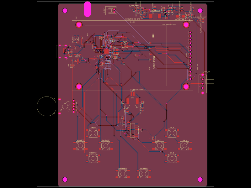 Similar packageabse/gameboyThis code defines the hardware mapping and schematic connections for a Raspberry Pi Pico-based development board featuring RP2040 microcontroller, USB-C connector, various power regulation components, decoupling capacitors, resistors, LEDs, headers, and supporting passive components for signal integrity and debugging.
 Discover something newimrishabh18/fitness_watchThis circuit integrates an ESP-12E microcontroller with various sensors, relays, and power management components, including an AO3400A transistor for switching loads, to enable wireless control and sensing functions.