seveibar/HS91L02W2C01
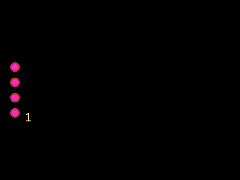
"A 4-pin HS91L02W2C01 I2C sensor or communication chip with plated through-hole mounting" The summary captures the key physical characteristics: pin count, specific component type, and mounting style, based on the pin labels (SCL/SDA suggesting I2C), the footprint, and the component details.
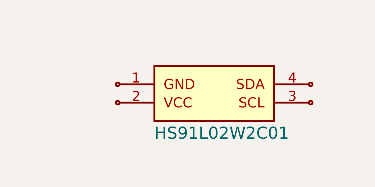
Usage: To import and use the HS91L02W2C01 component: 1. Import the component: ```tsx import { HS91L02W2C01 } from "@tsci/seveibar.HS91L02W2C01" ``` 2. Use in a circuit board: ```tsx <board> <HS91L02W2C01 name="U1" /> </board> ``` Available pins: - pin1: GND - pin2: VCC - pin3: SCL - pin4: SDA Supports positioning, naming, and tracing like other tscircuit components.
- Version
- 0.0.1
- License
- unset
- Stars
- 2
dist/pcb.svg
PCB
Schematic
<svg xmlns="http://www.w3.org/2000/svg" width="800" height="600" data-software-used-string="@tscircuit/core@0.0.747"><style></style><rect class="boundary" x="0" y="0" fill="#000" width="800" height="600" data-type="pcb_background" data-pcb-layer="global"/><rect class="pcb-boundary" fill="none" stroke="#fff" stroke-width="0.3" x="20.000038000072223" y="180.00001200002401" width="759.9999239998555" height="239.99997599995197" data-type="pcb_boundary" data-pcb-layer="global"/><g data-type="pcb_plated_hole" data-pcb-layer="through"><circle class="pcb-hole-outer" fill="rgb(200, 52, 52)" cx="50.00003500006679" cy="376.2001447802743" r="15.999998399997018" data-type="pcb_plated_hole" data-pcb-layer="top"/><circle class="pcb-hole-inner" fill="#FF26E2" cx="50.00003500006679" cy="376.2001447802743" r="9.999998999998137" data-type="pcb_plated_hole_drill" data-pcb-layer="drill"/></g><g data-type="pcb_plated_hole" data-pcb-layer="through"><circle class="pcb-hole-outer" fill="rgb(200, 52, 52)" cx="50.00003500006679" cy="325.4000482600914" r="15.999998399997018" data-type="pcb_plated_hole" data-pcb-layer="top"/><circle class="pcb-hole-inner" fill="#FF26E2" cx="50.00003500006679" cy="325.4000482600914" r="9.999998999998137" data-type="pcb_plated_hole_drill" data-pcb-layer="drill"/></g><g data-type="pcb_plated_hole" data-pcb-layer="through"><circle class="pcb-hole-outer" fill="rgb(200, 52, 52)" cx="50.00003500006679" cy="274.5999517399086" r="15.999998399997018" data-type="pcb_plated_hole" data-pcb-layer="top"/><circle class="pcb-hole-inner" fill="#FF26E2" cx="50.00003500006679" cy="274.5999517399086" r="9.999998999998137" data-type="pcb_plated_hole_drill" data-pcb-layer="drill"/></g><g data-type="pcb_plated_hole" data-pcb-layer="through"><circle class="pcb-hole-outer" fill="rgb(200, 52, 52)" cx="50.00003500006679" cy="223.79985521972344" r="15.999998399997018" data-type="pcb_plated_hole" data-pcb-layer="top"/><circle class="pcb-hole-inner" fill="#FF26E2" cx="50.00003500006679" cy="223.79985521972344" r="9.999998999998137" data-type="pcb_plated_hole_drill" data-pcb-layer="drill"/></g><path class="pcb-silkscreen pcb-silkscreen-top" d="M 20.000038000072223 180.00001200002401 L 779.9999619999277 180.00001200002401 L 779.9999619999277 419.999987999976 L 20.000038000072223 419.999987999976 L 20.000038000072223 180.00001200002401 Z" fill="none" stroke="#f2eda1" stroke-width="2.0000038000072276" stroke-linecap="round" stroke-linejoin="round" data-pcb-component-id="pcb_component_0" data-pcb-silkscreen-path-id="pcb_silkscreen_path_0" data-type="pcb_silkscreen_path" data-pcb-layer="top"/><text x="0" y="0" dx="0" dy="0" fill="#f2eda1" font-family="Arial, sans-serif" font-size="40.00007600014455" text-anchor="start" dominant-baseline="text-after-edge" transform="matrix(1,0,0,1,83.18265804704862,413.5382157226089)" class="pcb-silkscreen-text pcb-silkscreen-top" data-pcb-silkscreen-text-id="pcb_component_0" stroke="none" data-type="pcb_silkscreen_text" data-pcb-layer="top">1</text></svg>Related Packages
 More from this authorseveibar/wifi-test-board-1
 Similar packageabse/keypadThis code defines hardware components for a 4-pin I2C display header with plated through-hole pins and key connection labels, along with an ECG encoder module featuring multiple pins, footprints, and silkscreen paths for PCB mounting.
 Discover something newmuse/book-reading-clip-lampA 60‑mm ESP32‑S3 lamp-head controller PCB integrating USB‑C/battery charging and 3.3‑V power, OV5640 camera, I²S microphone and speaker amplifier, boost-driven six‑LED reading light, tactile controls, status indicators, and protection circuitry.