rushabhcodes/sbc_allwinner_v3s
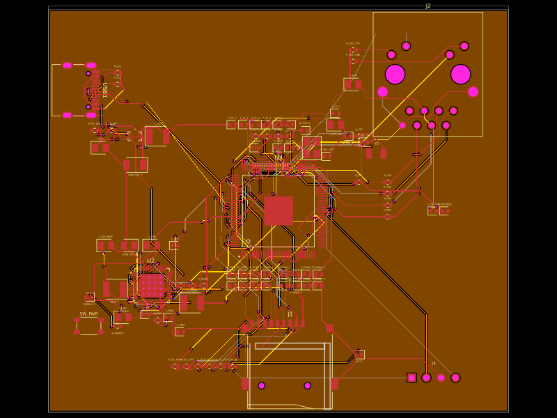
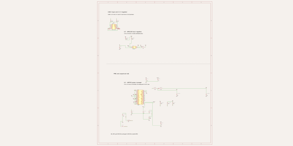
A 5 V USB‑C–powered Allwinner V3s embedded board with AXP203/AP61100 power regulation, microSD boot, UART, RTC/main clocks, USB device, and 10/100 Ethernet via an integrated-magnetics RJ45.
- Version
- 0.0.11
- License
- unset
- Stars
- 0
index.circuit.tsx
PCB
Schematic
import React from "react"
import { V3s } from "./imports/V3s"
import { AXP203 } from "./imports/AXP203"
import { AP61100Z6_7 } from "./imports/AP61100Z6_7"
import { TF_01A } from "./imports/TF_01A"
import { J0011D21BNL } from "./imports/J0011D21BNL"
import { X322524MOB4SI } from "./imports/X322524MOB4SI"
import { Q13FC13500004 } from "./imports/Q13FC13500004"
import { TYPE_C_31_M_12 } from "./imports/TYPE_C_31_M_12"

// Minimal stand-alone V3s: 5 V USB-C input, microSD boot, UART0, 10/100 RJ45.
// The imported packages retain their manufacturer pad numbering. All SoC
// connections below use physical pin numbers checked against the source KiCad
// netlist; pin 129 is the exposed ground pad.
const nets: Record<string, string[]> = {
  GND: [
    "U1.pin116", "U1.pin129", "U2.pin9", "U2.pin16", "U2.pin22",
    "U2.pin46", "U2.pin49", "U2.pin4", "U2.pin29", "U3.pin2",
    "J1.pin6", "J1.pin10", "J1.pin11", "J1.pin12", "J1.pin13",
    "J2.pin8", "J2.pin13", "J2.pin14", "USB1.pin1", "USB1.pin2",
    "USB1.pin3", "USB1.pin4", "USB1.pin13", "USB1.pin14",
    "Y1.pin2", "Y1.pin4", "J4.pin3",
  ],
  V5: ["USB1.pin15", "USB1.pin16", "U2.pin31", "U3.pin3", "U3.pin5"],
  IPS: ["U2.pin7", "U2.pin13", "U2.pin14", "U2.pin21", "U2.pin34", "U2.pin35", "U2.pin40", "U2.pin44"],
  V1V2: [
    "U2.pin10", "U1.pin19", "U1.pin20", "U1.pin21", "U1.pin25",
    "U1.pin26", "U1.pin38", "U1.pin47", "U1.pin51", "U1.pin56",
    "U1.pin58", "U1.pin64", "U1.pin80", "U1.pin88", "U1.pin108", "U1.pin126",
  ],
  V1V8: [
    "U2.pin17", "U1.pin59", "U1.pin60", "U1.pin61", "U1.pin62",
    "U1.pin65", "U1.pin66", "U1.pin67", "U1.pin68", "U1.pin69",
    "U1.pin70", "U1.pin72", "U1.pin79", "R_SV_TOP.pin1",
  ],
  V3V3: [
    "U3.pin6", "U1.pin12", "U1.pin29", "U1.pin50", "U1.pin57",
    "U1.pin85", "U1.pin93", "U1.pin104", "U1.pin109", "U1.pin122",
    "U1.pin127", "J1.pin4", "J4.pin1", "R_FB_TOP.pin1",
    "R_SD_CMD.pin1", "R_SD_D0.pin1", "R_SD_D1.pin1", "R_SD_D2.pin1",
    "R_SD_D3.pin1", "R_RSB_SCL.pin1", "R_RSB_SDA.pin1",
    "R_RESET.pin1", "R_LED_LINK.pin1", "R_LED_SPD.pin1", "L_ETH.pin1",
  ],
  V3V0: ["U2.pin12", "U1.pin76", "U1.pin115"],
  V3V3_RTC: ["U2.pin28", "U1.pin98"],
  VINT: ["U2.pin26", "U2.pin27"],
  RESET: ["U2.pin25", "U1.pin99", "R_RESET.pin2"],
  RSB_SCL: ["U2.pin2", "U1.pin46", "R_RSB_SCL.pin2"],
  RSB_SDA: ["U2.pin1", "U1.pin45", "R_RSB_SDA.pin2"],
  SD_CLK: ["J1.pin5"],
  SD_CMD: ["U1.pin103", "J1.pin3", "R_SD_CMD.pin2"],
  SD_D0: ["U1.pin106", "J1.pin7", "R_SD_D0.pin2"],
  SD_D1: ["J1.pin8", "R_SD_D1.pin2"],
  SD_D2: ["U1.pin101", "J1.pin1", "R_SD_D2.pin2"],
  SD_D3: ["U1.pin102", "J1.pin2", "R_SD_D3.pin2"],
  SD_CD: ["U1.pin100", "J1.pin9", "R_SD_CD.pin2"],
  UART_TX: ["U1.pin48", "J4.pin2"],
  UART_RX: ["U1.pin49", "J4.pin4"],
  USB_DM: ["USB1.pin7", "USB1.pin9", "U1.pin110"],
  USB_DP: ["USB1.pin8", "USB1.pin10", "U1.pin111"],
  CC1: ["USB1.pin6", "R_CC1.pin1"],
  CC2: ["USB1.pin12", "R_CC2.pin1"],
  X24_IN: ["Y1.pin3"],
  X24_OUT: ["Y1.pin1"],
  X32_IN: ["U1.pin96", "Y2.pin2", "R_X32.pin1"],
  X32_OUT: ["U1.pin95", "Y2.pin1", "R_X32.pin2"],
  SVREF: ["U1.pin63", "U1.pin71", "R_SV_TOP.pin2", "R_SV_BOT.pin1"],
  VRA1: ["U1.pin117"],
  VRA2: ["U1.pin118", "R_VRA2.pin1"],
  RTC_VIO: ["U1.pin97"],
  SZQ: ["U1.pin73", "R_SZQ.pin1"],
  EPHY_RTX: ["U1.pin94", "R_RTX.pin1"],
  TX_P: ["U1.pin92", "R_TXP.pin1"],
  TX_N: ["U1.pin91", "R_TXN.pin1"],
  RX_P: ["U1.pin90", "R_RXP.pin1"],
  RX_N: ["U1.pin89", "R_RXN.pin1"],
  JACK_TX_P: ["R_TXP.pin2", "J2.pin1"],
  JACK_TX_N: ["R_TXN.pin2", "J2.pin2"],
  JACK_RX_P: ["R_RXP.pin2", "J2.pin3"],
  JACK_RX_N: ["R_RXN.pin2", "J2.pin6"],
  ETH_BIAS: ["L_ETH.pin2", "J2.pin4", "J2.pin5"],
  LINK_LED: ["U1.pin77", "J2.pin10"],
  SPD_LED: ["J2.pin11"],
  LINK_LED_A: ["R_LED_LINK.pin2", "J2.pin9"],
  SPD_LED_A: ["R_LED_SPD.pin2", "J2.pin12"],
  LX2: ["U2.pin8", "L_CORE.pin1"],
  LX3: ["U2.pin15", "L_DRAM.pin1"],
  LX_3V3: ["U3.pin4", "L_3V3.pin1"],
  FB_3V3: ["U3.pin1", "R_FB_TOP.pin2", "R_FB_BOT.pin1"],
  PWRON: ["R_PWRON.pin1"],
  PWRON_BUTTON: ["R_PWRON.pin2", "SW_PWR.pin2"],
}

const resistors = [
  ["R_FB_TOP", "900k", -29, 14], ["R_FB_BOT", "200k", -27, 14],
  ["R_SD_CMD", "47k", 0, -29], ["R_SD_D0", "47k", 2, -29],
  ["R_SD_D1", "47k", 4, -29], ["R_SD_D2", "47k", 6, -29],
  ["R_SD_D3", "47k", 8, -29], ["R_SD_CD", "47k", 10, -29],
  ["R_RSB_SCL", "1.8k", -17, -14], ["R_RSB_SDA", "1.8k", -15, -14],
  ["R_RESET", "47k", -13, -14], ["R_PWRON", "1k", -28, -20],
  ["R_BIAS", "200k", -21, -19],
  ["R_SV_TOP", "2.2k", -4, 13], ["R_SV_BOT", "2.2k", -2, 13],
  ["R_VRA2", "200k", 0, 13], ["R_SZQ", "240", 2, 13],
  ["R_RTX", "6.04k", 19, 11], ["R_X32", "10M", 14, 13],
  ["R_TXP", "51", 19, 5], ["R_TXN", "51", 19, 3],
  ["R_RXP", "51", 19, 1], ["R_RXN", "51", 19, -1],
  ["R_LED_LINK", "330", 23, 15], ["R_LED_SPD", "330", 25, 15],
  ["R_CC1", "5.1k", -34, 20], ["R_CC2", "5.1k", -32, 20],
] as const

const capacitors: [string, string, number, number, string][] = [
  ["C_IN", "10uF", -31, 11, "V5"],
  ["C_IPS", "10uF", -27, -17, "IPS"],
  ["C_VINT", "1uF", -23, -17, "VINT"],
  ["C_BIAS", "1uF", -21, -17, "BIAS"],
  ["C_VREF", "1uF", -17, -21, "VREF"],
  ["C_PWRON", "100nF", -30, -18, "PWRON"],
  ["C_1V2_BULK", "10uF", -30, -6, "V1V2"],
  ["C_1V8_BULK", "10uF", -26, -6, "V1V8"],
  ["C_3V3_BULK", "22uF", -25, 8, "V3V3"],
  ["C_3V0", "4.7uF", -22, -6, "V3V0"],
  ["C_RTC", "1uF", -18, -6, "V3V3_RTC"],
  ["C_SD", "1uF", 14, -25, "V3V3"],
  ["C_X24_IN", "22pF", 7, 13, "X24_IN"],
  ["C_X24_OUT", "22pF", 10, 17, "X24_OUT"],
  ["C_X32_IN", "22pF", 14, 17, "X32_IN"],
  ["C_X32_OUT", "22pF", 16, 17, "X32_OUT"],
  ["C_SVREF", "100nF", -4, 11, "SVREF"],
  ["C_VRA1", "1uF", 0, 11, "VRA1"],
  ["C_VRA2", "1uF", 2, 11, "VRA2"],
  ["C_RTC_VIO", "4.7uF", 5, 11, "RTC_VIO"],
  ["C_ETH_BIAS", "100nF", 27, 0, "ETH_BIAS"],
  ["C_ETH_BULK", "1uF", 29, 0, "ETH_BIAS"],
  ...Array.from({ length: 8 }, (_, i): [string, string, number, number, string] => [
    `C_CORE_${i + 1}`, "1uF", -8 + (i % 4) * 2, -11 - Math.floor(i / 4) * 2, "V1V2",
  ]),
  ...Array.from({ length: 8 }, (_, i): [string, string, number, number, string] => [
    `C_DRAM_${i + 1}`, "1uF", 1 + (i % 4) * 2, -11 - Math.floor(i / 4) * 2, "V1V8",
  ]),
  ...Array.from({ length: 7 }, (_, i): [string, string, number, number, string] => [
    `C_IO_${i + 1}`, "1uF", -8 + i * 2, 15, "V3V3",
  ]),
]

// PCB locations near edge connectors differ from the functional schematic rows.
const resistorPcb: Record<string, [number, number]> = {
  R_FB_TOP: [-32, 14], R_FB_BOT: [-29, 14],
  R_SD_CMD: [-18, -27], R_SD_D0: [-16, -27],
  R_SD_D1: [-14, -27], R_SD_D2: [-12, -27],
  R_SD_D3: [-10, -27], R_SD_CD: [-8, -27],
  R_CC1: [-28, 22], R_CC2: [-28, 24],
  R_RSB_SCL: [-17, -13], R_RSB_SDA: [-15, -13], R_RESET: [-13, -13],
  R_RTX: [14, 5], R_LED_LINK: [13, 26], R_LED_SPD: [13, 28],
}

const capacitorPcb: Record<string, [number, number]> = {
  C_IPS: [-27, -18.5], C_VINT: [-23, -18],
  C_BIAS: [-19, -18.5], C_PWRON: [-33, -15],
  C_X24_IN: [4.5, 14], C_X24_OUT: [8.5, 9.5],
  C_X32_IN: [12, 13], C_X32_OUT: [15, 12],
  C_RTC_VIO: [10, 15],
  C_IO_7: [10, 17],
}

const capacitorSch: Record<string, [number, number]> = {
  C_1V2_BULK: [-11.6, -11], C_1V8_BULK: [-1.6, -11],
  C_3V3_BULK: [-5.6, 15], C_SD: [-2.4, 18.2],
  C_X24_IN: [6, 14],
  C_X32_IN: [13.3, 17], C_X32_OUT: [17.3, 17],
  ...Object.fromEntries(Array.from({ length: 8 }, (_, i) => [
    `C_CORE_${i + 1}`, [-11.6 + ((i + 1) % 3) * 1.6, -11 - Math.floor((i + 1) / 3) * 1.6],
  ])),
  ...Object.fromEntries(Array.from({ length: 8 }, (_, i) => [
    `C_DRAM_${i + 1}`, [-1.6 + ((i + 1) % 3) * 1.6, -11 - Math.floor((i + 1) / 3) * 1.6],
  ])),
  ...Object.fromEntries(Array.from({ length: 7 }, (_, i) => [
    `C_IO_${i + 1}`, [-5.6 + ((i + 1) % 3) * 1.6, 15 + Math.floor((i + 1) / 3) * 1.6],
  ])),
}

const resistorSch: Record<string, [number, number]> = {
  R_RSB_SCL: [-17.23, -14], R_RSB_SDA: [-14.77, -14],
  R_LED_LINK: [22.94, 15], R_LED_SPD: [25.06, 15],
}

const inputResistors = new Set(["R_FB_TOP", "R_FB_BOT", "R_CC1", "R_CC2"])
const cpuResistors = new Set(["R_SV_TOP", "R_SV_BOT", "R_VRA2", "R_SZQ", "R_X32"])
const cpuCapacitors = new Set(["C_3V3_BULK", "C_SD"])
const sheetForSection: Record<string, string> = {
  input: "Power",
  pmic: "Power",
  cpu: "V3s",
  boot: "Boot and UART",
  uart: "Boot and UART",
  ethernet: "Ethernet",
}
const resistorSectionName = (name: string) =>
  inputResistors.has(name) ? "input" : cpuResistors.has(name) ? "cpu" :
  name.startsWith("R_SD") ? "boot" :
  name.startsWith("R_TX") || name.startsWith("R_RX") || name.startsWith("R_LED") || name === "R_RTX" ? "ethernet" : "pmic"
const capacitorSectionName = (name: string) =>
  name === "C_IN" ? "input" : cpuCapacitors.has(name) ? "cpu" :
  name.includes("ETH") ? "ethernet" :
  name.includes("CORE") || name.includes("DRAM") || name.includes("IO") || name.includes("X") || name.includes("SV") || name.includes("VRA") || name.includes("RTC_VIO") ? "cpu" : "pmic"

const pcbReverse = new Set([
  "R_RSB_SCL", "R_RSB_SDA", "R_SZQ", "C_3V3_BULK",
  "C_SD", "C_X24_IN", "C_X32_IN", "C_1V8_BULK", "C_DRAM_2", "C_DRAM_6", "C_IO_6", "C_PWRON",
])

const powerSchematicY = (sectionName: string, y: number) =>
  y + (sectionName === "pmic" ? 6 : 0)

export default function MinimalV3sEthernet({ routingDisabled = false }: { routingDisabled?: boolean } = {}) {
  // Keep manual schematic coordinates fixed across sheets.
  return (
    <board width="80mm" height="70mm" layers={4} routingDisabled={routingDisabled} schLayout={{ layoutMode: "relative" }}>
      <copperpour connectsTo="net.GND" layer="inner1" clearance="0.15mm" boardEdgeMargin="0.25mm" />
      <schematicsheet name="Power" displayName="Power input and PMIC" sheetIndex={0} sheetWidth="360mm" sheetHeight="450mm">
        <schematicsection name="input" />
        <schematicsection name="pmic" />
        <schematictext text="USB-C input and 3.3 V regulator" schX={-35} schY={23} fontSize={0.4} anchor="left" />
        <schematictext text="USB1 is a 5 V sink; CC1 and CC2 each have a 5.1 kΩ pull-down." schX={-35} schY={22.2} fontSize={0.3} anchor="left" />
        <schematictext text="PMIC and sequenced rails" schX={-33} schY={2} fontSize={0.4} anchor="left" />
        <schematictext text="U2 - AXP203 power manager" schX={-29.5} schY={-1} fontSize={0.4} anchor="left" />
        <schematictext text="5 V in; 1.2 V core, 1.8 V DRAM, 3.0 V analog and 3.3 V RTC rails." schX={-29.5} schY={-1.6} fontSize={0.3} anchor="left" />
        <schematictext text="U3 - AP61100 buck regulator" schX={-29.5} schY={16.3} fontSize={0.4} anchor="left" />
        <schematictext text="5 V to 3.3 V for I/O, microSD and Ethernet LEDs." schX={-29.5} schY={15.7} fontSize={0.3} anchor="left" />
        <schematictext text="SW_PWR pulls PWRON low through R_PWRON to start the PMIC." schX={-34} schY={-18.5} fontSize={0.3} anchor="left" />
      </schematicsheet>
      <schematicsheet name="V3s" displayName="V3s and clocks" sheetIndex={1} sheetWidth="400mm" sheetHeight="390mm">
        <schematicsection name="cpu" />
        <schematictext text="V3s, clocks and decoupling" schX={-11} schY={23.5} fontSize={0.4} anchor="left" />
        <schematictext text="U1 - Allwinner V3s SoC" schX={-11} schY={22.8} fontSize={0.4} anchor="left" />
        <schematictext text="1.2 V core, 1.8 V DRAM and 3.3 V I/O; integrated DDR2." schX={-11} schY={22.2} fontSize={0.3} anchor="left" />
        <schematictext text="Boots from microSD; USB device/FEL and 10/100 Ethernet PHY." schX={-11} schY={21.7} fontSize={0.3} anchor="left" />
        <schematictext text="Y1 provides the 24 MHz main clock with 12 pF load capacitance." schX={7} schY={9.8} fontSize={0.3} anchor="left" />
        <schematictext text="Y2 - 32.768 kHz RTC crystal" schX={10.5} schY={18.1} fontSize={0.4} anchor="left" />
      </schematicsheet>
      <schematicsheet name="Ethernet" displayName="10/100 Ethernet" sheetIndex={2} sheetWidth="260mm" sheetHeight="240mm">
        <schematicsection name="ethernet" />
        <schematictext text="10/100 Ethernet with RJ45 magnetics" schX={20} schY={19} fontSize={0.4} anchor="left" />
        <schematictext text="J2 - RJ45 with integrated magnetics" schX={25} schY={8.5} fontSize={0.4} anchor="left" />
        <schematictext text="10/100BASE-T; 3.3 V LED supply" schX={25} schY={7.9} fontSize={0.3} anchor="left" />
        <schematictext text="51 Ω EPHY series resistors; 6.04 kΩ RTX bias; filtered 3.3 V center taps." schX={18} schY={-3.2} fontSize={0.3} anchor="left" />
      </schematicsheet>
      <schematicsheet name="Boot and UART" displayName="Boot and UART" sheetIndex={3} sheetWidth="400mm" sheetHeight="100mm">
        <schematicsection name="boot" />
        <schematicsection name="uart" />
        <schematictext text="microSD boot" schX={-2} schY={-23.5} fontSize={0.4} anchor="left" />
        <schematictext text="J1 boots SDC0 in 4-bit mode; CMD and data have 47 kΩ pull-ups." schX={-2} schY={-24.2} fontSize={0.3} anchor="left" />
        <schematictext text="UART debug" schX={24} schY={-24.5} fontSize={0.4} anchor="left" />
        <schematictext text="J4 exposes 3.3 V UART0 TX/RX and ground." schX={24} schY={-25.2} fontSize={0.3} anchor="left" />
      </schematicsheet>

      <V3s name="U1" pcbX={0} pcbY={0} schX={0} schY={0} schSectionName="cpu" schSheetName="V3s" />
      <AXP203 name="U2" pcbX={-22} pcbY={-13} schX={-24} schY={-6} schHeight={5} schSectionName="pmic" schSheetName="Power" />
      <AP61100Z6_7 name="U3" pcbX={-25} pcbY={13} schX={-26} schY={11} schSectionName="input" schSheetName="Power" />
      <TF_01A name="J1" pcbX={2} pcbY={-25} schX={0} schY={-27} schHeight={1.4} schSectionName="boot" schSheetName="Boot and UART" />
      <J0011D21BNL name="J2" pcbX={26} pcbY={21.8} schX={26} schY={4} schSectionName="ethernet" schSheetName="Ethernet" />
      <TYPE_C_31_M_12 name="USB1" pcbX={-34} pcbY={21} pcbRotation={-90} schX={-33} schY={18} schSectionName="input" schSheetName="Power" />
      <pinheader name="J4" pinCount={4} pitch="2.54mm" gender="male" pcbX={27} pcbY={-29} schX={25} schY={-28} schSectionName="uart" schSheetName="Boot and UART" />
      <X322524MOB4SI name="Y1" loadCapacitance="12pF" pcbX={5.8} pcbY={11} pcbRotation={90} schX={9} schY={12} schSectionName="cpu" schSheetName="V3s" />
      <Q13FC13500004 name="Y2" pcbX={17} pcbY={10} schX={15.3} schY={17.3} schRotation={180} schSectionName="cpu" schSheetName="V3s" />
      <pushbutton name="SW_PWR" footprint="smdpushbutton" pcbX={-33} pcbY={-20} schX={-30} schY={-16} schSectionName="pmic" schSheetName="Power" />
      <inductor name="L_CORE" inductance="4.7uH" footprint="1210" pcbX={-28.5} pcbY={-13.6} pcbRotation={180} schX={-19} schY={-3} schSectionName="pmic" schSheetName="Power" />
      <inductor name="L_DRAM" inductance="4.7uH" footprint="1210" pcbX={-15} pcbY={-16} schX={-17} schY={-3} schSectionName="pmic" schSheetName="Power" />
      <inductor name="L_3V3" inductance="1uH" footprint="1210" pcbX={-21} pcbY={13} schX={-23} schY={11} schSectionName="input" schSheetName="Power" />
      <inductor name="L_ETH" inductance="10uH" footprint="0805" pcbX={13} pcbY={22} schX={24} schY={12} schSectionName="ethernet" schSheetName="Ethernet" />
      {resistors.map(([name, resistance, x, y]) => (
        <resistor key={name} name={name} resistance={resistance} footprint="0402" pcbX={resistorPcb[name]?.[0] ?? x} pcbY={resistorPcb[name]?.[1] ?? y} pcbRotation={pcbReverse.has(name) ? 180 : 0} schX={resistorSch[name]?.[0] ?? x} schY={powerSchematicY(resistorSectionName(name), resistorSch[name]?.[1] ?? y)} schRotation={name.startsWith("R_TX") || name.startsWith("R_RX") || name === "R_X32" || name === "R_PWRON" ? 0 : -90} schSectionName={resistorSectionName(name)} schSheetName={sheetForSection[resistorSectionName(name)]} />
      ))}
      {capacitors.map(([name, capacitance, x, y, rail]) => (
        <React.Fragment key={name}>
          <capacitor name={name} capacitance={capacitance} footprint={capacitance === "22uF" ? "1206" : capacitance === "10uF" || capacitance === "4.7uF" ? "0805" : "0402"} pcbX={capacitorPcb[name]?.[0] ?? x} pcbY={capacitorPcb[name]?.[1] ?? y} pcbRotation={pcbReverse.has(name) ? 180 : 0} schX={capacitorSch[name]?.[0] ?? x} schY={powerSchematicY(capacitorSectionName(name), capacitorSch[name]?.[1] ?? y)} schRotation={-90} schSectionName={capacitorSectionName(name)} schSheetName={sheetForSection[capacitorSectionName(name)]} />
          <trace from={`${name}.pin1`} to={`net.${rail}`} />
          <trace from={`${name}.pin2`} to="net.GND" />
        </React.Fragment>
      ))}
      {Object.entries(nets).flatMap(([name, pins]) =>
        pins.map((pin) => (
          <React.Fragment key={`${name}:${pin}`}>
            <trace from={pin} to={`net.${name}`} />
          </React.Fragment>
        )),
      )}
      {/* Escape the adjacent V3s clock pads vertically before turning. */}
      <trace name="X24_IN_SOC" from="U1.pin75" to="Y1.pin3" pcbPath={[{ x: 2.2, y: 8.8 }, { x: 3.8, y: 10.2 }, { x: 3.8, y: 12.1 }]} />
      <trace name="X24_OUT_SOC" from="U1.pin74" to="Y1.pin1" pcbPath={[{ x: 2.6, y: 8.8 }, { x: 6.65, y: 8.8 }]} />
      <trace name="X24_IN_CAP" from="C_X24_IN.pin1" to="Y1.pin3" pcbPath={[{ x: -0.51, y: 0.6 }]} />
      <trace name="LX2_SWITCH" from="U2.pin8" to="L_CORE.pin1" pcbPath={[{ x: -4.2, y: -0.6 }]} />
      <trace name="LX3_SWITCH" from="U2.pin15" to="L_DRAM.pin1" pcbPath={[
        { x: -1.4, y: -3.8 }, { x: -1.4, y: -3.8, via: true, toLayer: "bottom" },
        { x: -1.4, y: -3.8 }, { x: -1.8, y: -4.8 }, { x: 4.5, y: -4.8 },
        { x: 4.5, y: -4.8, via: true, toLayer: "top" }, { x: 4.5, y: -4.8 },
      ]} />
      <trace name="USB_DM_SOC" from="U1.pin110" to="USB1.pin9" pcbPath={[
        { x: -9, y: 1 }, { x: -9, y: 1, via: true, toLayer: "inner2" },
        { x: -9, y: 1 }, { x: -23, y: 19 }, { x: -26.4, y: 19 },
        { x: -26.4, y: 19, via: true, toLayer: "top" }, { x: -26.4, y: 19 },
        { x: -29.5, y: 20.75 },
      ]} />
      <trace name="SD_CLK_SOC" from="U1.pin105" to="J1.pin5" pcbPath={[
        { x: -9.7, y: 3 }, { x: -9.7, y: 3, via: true, toLayer: "bottom" },
        { x: -9.7, y: 3 },
        { x: -10, y: -6 }, { x: -0.914, y: -13.897 },
        { x: -0.914, y: -13.897, via: true, toLayer: "top" },
        { x: -0.914, y: -13.897 },
      ]} />
      <trace name="SD_D1_SOC" from="U1.pin107" to="J1.pin8" pcbPath={[
        { x: -11, y: 2.2 }, { x: -11, y: 2.2, via: true, toLayer: "bottom" },
        { x: -11, y: 2.2 }, { x: -11, y: -8 }, { x: -3.46, y: -15 },
        { x: -3.46, y: -17.5 }, { x: -3.46, y: -17.5, via: true, toLayer: "top" },
        { x: -3.46, y: -17.5 },
      ]} />
      <trace name="PWRON_PMIC" from="U2.pin47" to="C_PWRON.pin1" pcbPath={[
        { x: -1.8, y: 3.8 }, { x: -5.5, y: 3.8 },
        { x: -10, y: 3.8 }, { x: -10, y: -2 },
      ]} />
      <trace name="SPD_LED_SOC" from="U1.pin78" to="J2.pin11" pcbPath={[
        { x: 1, y: 9.4 }, { x: 1, y: 9.4, via: true, toLayer: "bottom" },
        { x: 1, y: 9.4 }, { x: 8, y: 16 }, { x: 13, y: 23 },
        { x: 17, y: 31 }, { x: 22.2149, y: 31 },
      ]} />
      <trace from="R_CC1.pin2" to="net.GND" />
      <trace from="R_CC2.pin2" to="net.GND" />
      <trace from="L_CORE.pin2" to="net.V1V2" />
      <trace from="L_DRAM.pin2" to="net.V1V8" />
      <trace from="L_3V3.pin2" to="net.V3V3" />
      <trace from="R_FB_BOT.pin2" to="net.GND" />
      <trace from="R_SD_CD.pin1" to="net.V3V3" />
      <trace from="R_SV_BOT.pin2" to="net.GND" />
      <trace from="R_VRA2.pin2" to="net.GND" />
      <trace from="R_SZQ.pin2" to="net.GND" />
      <trace from="R_RTX.pin2" to="net.GND" />
      <trace from="R_BIAS.pin1" to="net.BIAS" />
      <trace from="R_BIAS.pin2" to="net.GND" />
      <trace from="U2.pin23" to="net.BIAS" />
      <trace from="U2.pin24" to="net.VREF" />
      <trace from="SW_PWR.pin1" to="net.GND" />
      <trace from="SW_PWR.pin3" to="net.GND" />
      <trace from="SW_PWR.pin4" to="net.PWRON_BUTTON" />
    </board>
  )
}
Related Packages
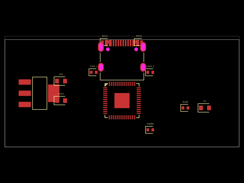 More from this authorrushabhcodes/RP2040A compact electronic circuit integrating a USB-C port, a voltage regulator (AMS1117 3.3V), a Raspberry Pi Pico RP2040 microcontroller, supporting power management, voltage regulation, and USB connectivity with associated passive components.
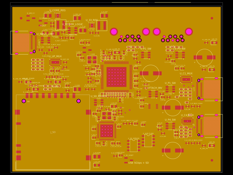 Similar packagegokul/usb3-sd-hubEngineering draft: four-layer, computer-powered USB 3 hub with one USB-C host socket, two USB-C and two USB-A accessory sockets, and a full-size SD slot. Board and three schematic previews are available. Routing and production checks are incomplete; not fabrication ready.
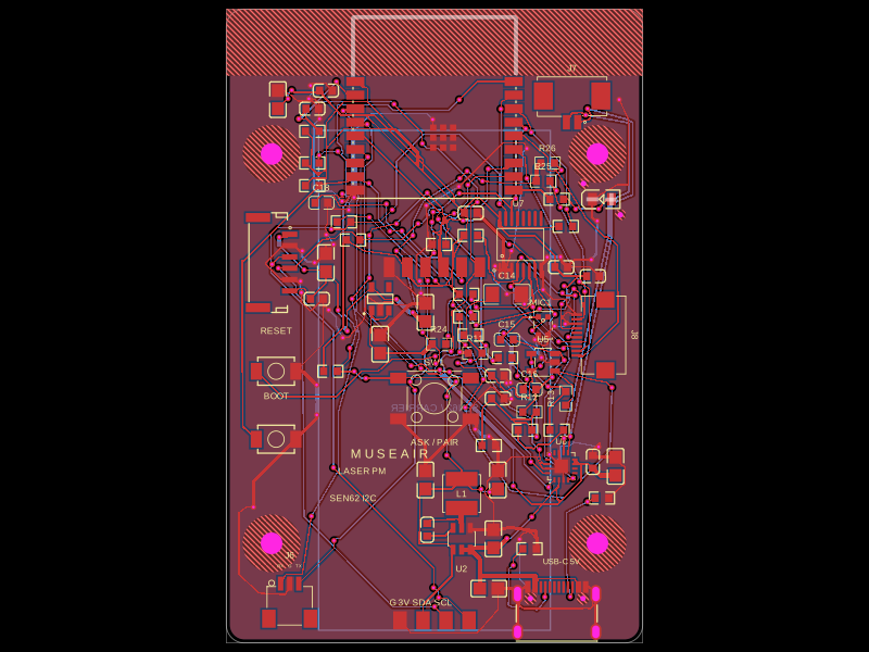 Discover something newabse/museair-usbUSB-C–powered ESP32-C3 controller board with AP63203 buck conversion, AP2112K 3.3V regulation, I²C SEN62 sensor interface, status LED, buttons, UART/I²C headers, and extensive decoupling.