rushabhcodes/sbc_allwinner_v3s
A 5 V USB‑C–powered Allwinner V3s embedded board with AXP203/AP61100 power regulation, microSD boot, UART, RTC/main clocks, USB device, and 10/100 Ethernet via an integrated-magnetics RJ45.
- Version
- 0.0.11
- License
- unset
- Stars
- 0
README.md
# Minimal Allwinner V3s SBC with RJ45

This is a tscircuit implementation of a reduced [vd-rd V3s SBC](https://github.com/vd-rd/sbc_allwinner_v3s). It keeps the V3s, microSD boot, 24 MHz and 32.768 kHz clocks, UART0 debug, USB-C 5 V input, and onboard 10/100 Ethernet. Wi-Fi, LCD, audio connectors, battery charging, SPI flash, and expansion headers are omitted.

The RJ45 is a Pulse **J0011D21BNL** with integrated 1:1 magnetics and LEDs. The four V3s EPHY data pins connect through 51 Ω series resistors to the jack's PCB-side transformer pins. Both center taps share a filtered 3.3 V bias. EPHY-RTX has a 6.04 kΩ resistor to ground. The jack pin map follows the [Pulse J403 datasheet](https://productfinder.pulseelectronics.com/api/open/part-attachments/datasheet/j0011d21bnl).

## Power and boot

| Rail | Source | Loads |
| --- | --- | --- |
| 5 V | USB-C sink, two 5.1 kΩ CC pull-downs | AXP203 VBUS, 3.3 V buck |
| 3.3 V | AP61100 buck | V3s I/O/EPHY, microSD, RJ45 LEDs |
| 3.0 V | AXP203 LDO2 | V3s AVCC and PLL |
| 1.8 V | AXP203 DCDC3, DC3SET grounded | V3s internal DDR2 |
| 1.2 V | AXP203 DCDC2 | V3s CPU, SYS, and EPHY core |
| RTC 3.3 V | AXP203 LDO1, LDO1SET to VINT | V3s RTC |

The original reference netlist labels a 1.8 V DRAM rail but leaves it without a supply. This version deliberately feeds it from DCDC3. CPU and SYS share one 1.2 V rail to minimize the power system, so dynamic voltage scaling is outside the scope of this version.

The imported V3s package is the exposed-pad LQFP-128-EP variant. `index.circuit.tsx` uses physical pad numbers from the reference KiCad schematic. The microSD slot is wired to SDC0 (PF0–PF5) with card detect on PF6. UART0 uses PB8/PB9. The USB-C data pair also reaches the V3s USB controller for device/FEL recovery.

## Build

```sh
bun install
bun run build
```

The default build routes all 56 nets on an 80 × 70 mm canvas, then trims an unused 4 mm strip from the right edge. The final four-layer PCB is **76 × 70 mm** in `dist/compact/circuit.json`; the source preview shows the larger routing canvas. The trim also updates the inner-layer ground pour and checks that no trace or component courtyard crosses the new edge. Check the final board with `bunx tsci check shorts dist/compact/circuit.json` and `bunx tsci check placement dist/compact/circuit.json`. Routing fixes include direct top-layer 24 MHz crystal traces, a short LX2 switch trace beside the PMIC, and controlled SD, LX3, and USB_DM escapes.

PCB snapshots from the passing compact build: [full board](./pcb-routed.png), [Ethernet to RJ45](./pcb-ethernet.png), and [clock, power, SD, and USB nets](./pcb-critical-nets.png). Rebuild with `bun run build`; the autorouter can take several minutes. Run `bunx tsci check shorts dist/compact/circuit.json` after any routing change.

The schematic uses four sheets: [Power input and PMIC](./schematic-sheets/power.png), [V3s and clocks](./schematic-sheets/v3s.png), [Ethernet and RJ45](./schematic-sheets/ethernet.png), and [microSD boot and UART](./schematic-sheets/boot-uart.png). Each sheet includes short notes explaining its main components, supply rails, or interface signals. A [stacked overview](./schematic-review.png) shows all four. Cross-sheet nets use matching labels, while the PCB remains one routed board.

This is a routed prototype, not a released fabrication package. The part-selection engine reports 0402 supplier footprint discrepancies and cannot resolve the selected 22 pF capacitor's JLCPCB number, so verify or replace those parts before assembly. Also verify the ordered AXP203 variant's startup voltages and timing, USB-C connector orientation and power budget, and Ethernet center-tap/EMC network.

## Imported parts

The V3s, AXP203, AP61100, TF-01A microSD slot, J0011D21BNL RJ45, TYPE-C-31-M-12 USB receptacle, and both crystals were imported with `tsci import --jlcpcb`. Their generated components and footprints are kept in [`imports`](./imports).
Related Packages
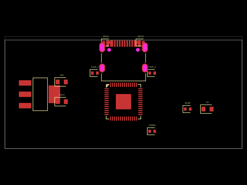 More from this authorrushabhcodes/RP2040A compact electronic circuit integrating a USB-C port, a voltage regulator (AMS1117 3.3V), a Raspberry Pi Pico RP2040 microcontroller, supporting power management, voltage regulation, and USB connectivity with associated passive components.
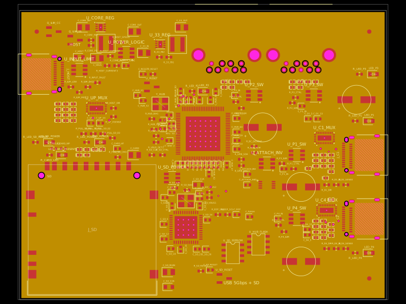 Similar packagegokul/usb3-sd-hubEngineering draft: four-layer, computer-powered USB 3 hub with one USB-C host socket, two USB-C and two USB-A accessory sockets, and a full-size SD slot. Board and three schematic previews are available. Routing and production checks are incomplete; not fabrication ready.
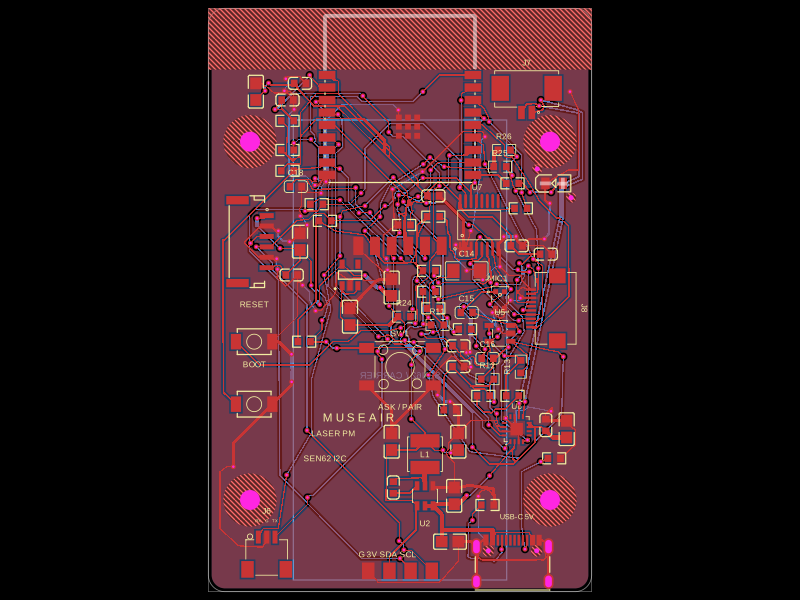 Discover something newabse/museair-usbUSB-C–powered ESP32-C3 controller board with AP63203 buck conversion, AP2112K 3.3V regulation, I²C SEN62 sensor interface, status LED, buttons, UART/I²C headers, and extensive decoupling.