rushabhcodes/fidget-counter
A tscircuit package created by rushabhcodes.
- Version
- 1.0.31
- License
- unset
- Stars
- 0
validation/kicad-review-adapter.py
"""KiCad9 review adapter: syntax and fill topology; never refill copper.

Union existing fragmented filled polygons, preserve every hole, and encode them
as native bridged contours. The independent checker enforces1nm copper parity,
the native integer-coordinate resolution. No electrical error is waived.
"""
from pathlib import Path
import json,re,sys,subprocess,shutil
import pcbnew
source=Path(sys.argv[1]);out=Path(sys.argv[2]);out.parent.mkdir(parents=True,exist_ok=True)
text=source.read_text();text,n=re.subn(r'\(tenting\s+\(front yes\)\s+\(back yes\)\s*\)','(tenting front back)',text)
out.write_text(text);b=pcbnew.LoadBoard(str(out))
zones=[]
def points_nm(v):return [[v.CPoint(i).x,v.CPoint(i).y]for i in range(v.PointCount())]
for zi,z in enumerate(b.Zones()):
 if z.GetIsRuleArea():continue
 p=z.GetFilledPolysList(z.GetLayer())
 zones.append({'zone_index':zi,'fragments':[{'outer':points_nm(p.COutline(i)),'holes':[points_nm(p.CHole(i,j))for j in range(p.HoleCount(i))]}for i in range(p.OutlineCount())]})
coalesced=json.loads(subprocess.check_output(['python',str(Path(__file__).with_name('coalesce-native-fills.py'))],input=json.dumps(zones),text=True))
for row in coalesced:
 z=list(b.Zones())[row['zone_index']];p=pcbnew.SHAPE_POLY_SET()
 for poly in row['polygons']:
  oi=p.NewOutline()
  for x,y in poly['outer']:p.Append(round(x),round(y),oi)
  for ring in poly['holes']:
   hi=p.NewHole(oi)
   for x,y in ring:p.Append(round(x),round(y),oi,hi)
 # Native files serialize filled outlines. Fracture bridges holes into those
 # outlines; omitting this step would silently fill the holes on serialization.
 p.Fracture();z.SetFilledPolysList(z.GetLayer(),p);z.SetNeedRefill(False);z.SetIsFilled(True)
out.with_suffix('.fill-topology.json').write_text(json.dumps({'method':'Union existing native fragments; preserve holes as bridged contours; no refill','native_coordinate_grid_nm':1,'zones':[{'zone_index':r['zone_index'],'fragments_before':r['fragments_before'],'contours_after':len(r['polygons'])}for r in coalesced]},indent=2)+'\n')
for z in b.Zones():
 if not z.GetIsRuleArea():z.SetLocalClearance(pcbnew.FromMM(.10))
pcbnew.SaveBoard(str(out),b)
profile={'board':{'design_settings':{'defaults':{},'diff_pair_dimensions':[],'drc_exclusions':[],'rules':{'min_clearance':.1,'min_track_width':.11,'min_via_diameter':.55,'min_through_hole_diameter':.3,'min_via_annular_width':.125,'min_copper_edge_clearance':.3,'min_hole_clearance':.2,'min_hole_to_hole':.2},'track_widths':[],'via_dimensions':[]}},'boards':[],'libraries':{'pinned_footprint_libs':[],'pinned_symbol_libs':[]},'meta':{'filename':out.with_suffix('.kicad_pro').name,'version':1},'net_settings':{'classes':[{'name':'Default','description':'JLC 2layer1oz minima; exact source fills retained without refill','clearance':.1,'track_width':.11,'via_diameter':.55,'via_drill':.3}],'meta':{'version':0}},'pcbnew':{'page_layout_descr_file':''},'sheets':[],'text_variables':{}}
out.with_suffix('.kicad_pro').write_text(json.dumps(profile,indent=2)+'\n')
out.with_suffix('.kicad_dru').write_text('''(version 1)
(rule "JLC different-net SMT pad spacing"
 (condition "A.Type == 'Pad' && B.Type == 'Pad' && A.Pad_Type == 'SMD' && B.Pad_Type == 'SMD'")
 (constraint clearance (min 0.15mm)))
''')
def fills(board):
 result=[]
 for z in board.Zones():
  if z.GetIsRuleArea():continue
  layer='top'if z.GetLayer()==pcbnew.F_Cu else'bottom';polys=z.GetFilledPolysList(z.GetLayer())
  def points(c):return [[c.CPoint(i).x/1e6-100,100-c.CPoint(i).y/1e6]for i in range(c.PointCount())]
  for i in range(polys.OutlineCount()):result.append({'net':z.GetNetname(),'layer':layer,'outer':points(polys.COutline(i)),'holes':[points(polys.CHole(i,j))for j in range(polys.HoleCount(i))]})
 return result
out.with_suffix('.fills.json').write_text(json.dumps(fills(b)))
def drc(path):
 result=subprocess.run(['kicad-cli','pcb','drc',str(path),'--format','json','--output',str(path.with_suffix('.drc.json'))],capture_output=True,text=True)
 path.with_suffix('.drc.log').write_text(result.stdout+result.stderr)
 assert path.with_suffix('.drc.json').exists(),result.stderr
drc(out)
# A real wrong-net short must survive this adapter and be rejected by the review.
bad=out.with_name(out.stem+'-negative.kicad_pcb');target=next(p for f in b.GetFootprints()if f.GetReference()=='U2'for p in f.Pads()if p.GetNumber()=='4')
t=pcbnew.PCB_TRACK(b);t.SetLayer(pcbnew.F_Cu);t.SetWidth(pcbnew.FromMM(.25));t.SetNetCode(b.GetNetcodeFromNetname('VBAT'));t.SetStart(target.GetPosition());t.SetEnd(pcbnew.VECTOR2I(target.GetPosition().x+1000000,target.GetPosition().y));b.Add(t)
pcbnew.SaveBoard(str(bad),b)
for suffix in ['.kicad_pro','.kicad_dru']:shutil.copyfile(out.with_suffix(suffix),bad.with_suffix(suffix))
drc(bad)
print(json.dumps({'review_board':str(out),'tenting_syntax_replacements':n,'copper_refilled':False,'injected_wrong_net_short':str(bad)}))
Related Packages
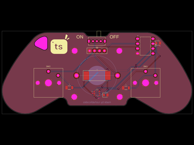 More from this authorrushabhcodes/Attiny85-Arcade-KeychainThis code defines a PCB and electronic component assembly for a compact ATtiny85-based gamepad keychain featuring power management, an OLED display, pushbutton inputs, audio piezo driver, and mechanical mounting, all mapped onto a custom PCB outline.
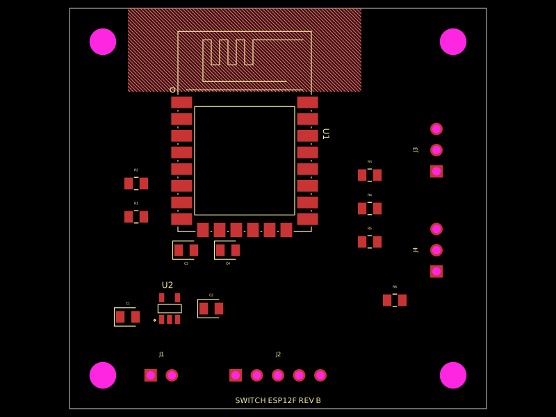 Discover something newhrithik18k/switch-pcb