rushabhcodes/fidget-counter
A tscircuit package created by rushabhcodes.
- Version
- 1.0.31
- License
- unset
- Stars
- 0
validation/check-native-fabrication.py
"""Audit actual KiCad fills and narrowly identify source/export semantic diagnostics."""
from pathlib import Path
import collections,csv,hashlib,io,json,math,sys,zipfile,runpy
from shapely.geometry import Polygon,Point,box,LineString
from shapely.ops import unary_union
R=Path(__file__).resolve().parents[1];D=Path(sys.argv[1]);c=json.loads((R/'published.circuit.json').read_text())
rf=runpy.run_path(str(R/'validation/check-nordic-rf.py'));rf_report=rf['verify'](c)
return_id=next(e['source_trace_id']for e in c if e['type']=='source_trace'and e.get('name')=='C3_VSS2_RETURN')
return_route=next(e['route']for e in c if e['type']=='pcb_trace'and e.get('source_trace_id')==return_id)
return_centerline=LineString([(p['x'],p['y'])for p in return_route])
def shape(e):
 b=e['brep_shape'];assert set(b)<= {'outer_ring','inner_rings'}
 return Polygon([(v['x'],v['y'])for v in b['outer_ring']['vertices']], [[(v['x'],v['y'])for v in h['vertices']]for h in b.get('inner_rings',[])]).buffer(0)
fresh=(R/'validation/fresh-routing-reference.json').exists()
components=lambda p:list(p.geoms)if hasattr(p,'geoms')else[p]
layers=['top','bottom'];pours={l:unary_union([shape(e)for e in c if e['type']=='pcb_copper_pour'and e['layer']==l])for l in layers}
f=json.loads((D/'review.fills.json').read_text());equivalence={}
def native_parity(expected,actual):
 # Union intersections can fall between integer native coordinates. Native
 # contour reconstruction may round by at most1nm; no coarser change is allowed.
 added=actual.difference(expected.buffer(.000001)).area
 removed=expected.difference(actual.buffer(.000001)).area
 assert added<1e-9 and removed<1e-9,('Native copper changed beyond1nm coordinate precision',added,removed)
for l in layers:
 assert all(p['net']=='GND'for p in f)
 native=unary_union([Polygon(p['outer'],p['holes']).buffer(0)for p in f if p['layer']==l]);delta=pours[l].symmetric_difference(native).area
 native_parity(pours[l],native)
 bad=native.difference(native.representative_point().buffer(.01))
 try:native_parity(pours[l],bad)
 except AssertionError:pass
 else:raise AssertionError('Native real-copper removal was accepted')
 equivalence[l]={'symmetric_difference_mm2':delta,'hausdorff_mm':pours[l].hausdorff_distance(native),'native_coordinate_tolerance_nm':1,'physical_regions':len(components(pours[l])),'source_area_mm2':pours[l].area,'export_fragments':sum(p['layer']==l for p in f),'negative_copper_removal_rejected':True}
# Ground conductor identity is derived electrically, never from proximity alone.
gn=next(e for e in c if e['type']=='source_net'and e['name']=='GND');key=gn['subcircuit_connectivity_map_key']
ports={e['pcb_port_id']:e for e in c if e['type']=='pcb_port'};sources={e['source_port_id']:e for e in c if e['type']=='source_port'};traces={e['source_trace_id']:e for e in c if e['type']=='source_trace'}
def ground(e):
 return e.get('subcircuit_connectivity_map_key',traces.get(e.get('source_trace_id'),{}).get('subcircuit_connectivity_map_key'))==key or sources.get(ports.get(e.get('pcb_port_id'),{}).get('source_port_id'),{}).get('subcircuit_connectivity_map_key')==key or e.get('connection_name')==gn['source_net_id']
conductors={l:[]for l in layers}
for e in c:
 if not ground(e):continue
 if e['type']=='pcb_trace':
  for a,b in zip(e['route'],e['route'][1:]):
   if a['route_type']==b['route_type']=='wire'and a['layer']==b['layer']:conductors[a['layer']].append(LineString([(a['x'],a['y']),(b['x'],b['y'])]).buffer(min(a['width'],b['width'])/2))
 elif e['type']=='pcb_via':
  for l in e['layers']:conductors[l].append(Point(e['x'],e['y']).buffer(e['outer_diameter']/2))
 elif e['type']=='pcb_smtpad':
  # Inscribed disc is conservative for all imported orthogonal/pill lands.
  conductors[e['layer']].append(Point(e['x'],e['y']).buffer((min(e['width'],e['height'])/2 if 'width'in e else e['radius'])))
contacts=[]
for l in layers:
 for p in components(pours[l]):
  n=sum(p.intersection(g).area>1e-9 for g in conductors[l]);assert n>0,(l,'Physical floating GND region',p.bounds)
  contacts.append({'layer':l,'area_mm2':p.area,'ground_conductor_contacts':n})
keepouts=[]
for k in c:
 if k['type']!='pcb_keepout':continue
 x,y=k['center']['x'],k['center']['y'];q=Point(x,y).buffer(k['radius'],resolution=256)if k['shape']=='circle'else box(x-k['width']/2,y-k['height']/2,x+k['width']/2,y+k['height']/2)
 rf_moat=k['shape']=='rect'and abs(k['center']['x']+2.9)<1e-6 and abs(k['center']['y']-5.415)<1e-6
 if k['shape']=='rect'and abs(k['center']['y']-15.8)>.01 and not rf_moat:
  assert not any(e['type']in ['pcb_via','pcb_plated_hole']and q.intersects(Point(e['x'],e['y']).buffer(e['hole_diameter']/2))for e in c),'Drill in reserved SMD-pad underside'
  keepouts.append({'id':k['pcb_keepout_id'],'purpose':'Via/drill exclusion under opposite-side SMD pad; GND fill is allowed','passed':True})
 else:
  for l in k['layers']:assert pours[l].intersection(q.buffer(-.015)).area<1e-7,(k['pcb_keepout_id'],l,'Actual fill intrudes into reserved area')
  keepouts.append({'id':k['pcb_keepout_id'],'actual_fill_clear':True,'polygonization_tolerance_mm':.015})
drc=json.loads((D/'review.drc.json').read_text());assert not drc['unconnected_items'],'Unconnected native copper'
holes=[e for e in c if e['type']=='pcb_hole']
def classify(e):
 descriptions=[i['description']for i in e['items']]
 if e['type']=='items_not_allowed'and len(descriptions)==1:
  d=descriptions[0];pos=e['items'][0]['pos'];x,y=pos['x']-100,100-pos['y']
  if d=='NPTH pad of 'and any(math.hypot(x-h['x'],y-h['y'])<1e-5 for h in holes):return 'mounting drill inside its own support/head keepout'
  if d in ['Zone [GND] on F.Cu','Zone [GND] on B.Cu']:return 'outline-based check; exact actual fills and keepouts independently verified'
  if (d=='Footprint ANT1'or d.startswith('Pad ')and ' of ANT1 'in d)and -3.5<=x<=3.5 and 13.6<=y<=18:return 'source excludes ANT1 from its RF keepout'
  if d.startswith('Track [.L2 > .pin2 to .ANT1 > .feed] on F.Cu')and -4<=x<=4.31 and 4.39<=y<=18:return 'intended ANT1 feed entry into RF keepout'
  if d.startswith('Track [GND] on F.Cu')and return_centerline.distance(Point(x,y))<1e-5:return 'intended isolated C3 return; actual source and native copper verified to contact general ground only through VSS31 land'
  if d.startswith('Track [.U1 > .ANT to .L1 > .pin1] on F.Cu')and -4.15<=x<=-1.65 and 4.93<=y<=5.9:return 'intended RF shunt branch in pour-exclusion region; source/native copper parity verified at1nm'
  if d in ['Footprint C3','Pad 1 [.U1 > .ANT to .L1 > .pin1] of C3 on F.Cu','Pad 2 [GND] of C3 on F.Cu']and -4.15<=x<=-1.65 and 4.93<=y<=5.9:return 'source explicitly excludes C3 from its local pour-exclusion region; both actual fills are clear'
  if d=='Footprint U1'and abs(x+7.5)<1e-6 and abs(y-5)<1e-6:return 'source explicitly excludes U1 courtyard from adjacent C3 pour-exclusion region; actual pads and return checked independently'
  if d in ['Pad 31 [GND] of U1 on F.Cu','Pad 32 [<no net>] of U1 on F.Cu']and abs(x+4.500006)<1e-6 and (abs(y-5.199898)<1e-6 or abs(y-5.599948)<1e-6):return 'source excludes U1 from adjacent pour-exclusion region; VSS31 return and unconnected DEC2/pin32 verified independently'
 if e['type']=='courtyards_overlap'and sorted(descriptions)==['Footprint C16','Footprint GPIO_SCL']:
  gpio=next(x for x in c if x['type']=='source_component'and x['name']=='GPIO_SCL');assert any(x['type']=='pcb_component'and x.get('source_component_id')==gpio['source_component_id']and x.get('do_not_place')for x in c);return 'DNP bare signal via courtyard; no assembled component body'
 return None
classified=[]
for e in drc['violations']:
 if e['severity']=='error':
  reason=classify(e);assert reason,('Unresolved native DRC error',e);classified.append({'diagnostic':e,'reason':reason})
 assert e['type']in ['items_not_allowed','courtyards_overlap','isolated_copper','lib_footprint_issues','silk_over_copper','text_height'],('New unreviewed native diagnostic',e)
assert 8<=len(classified)<=30,'Unexpected source/export exception count; review again'
negative=json.loads((D/'review-negative.drc.json').read_text())
assert any(e['type']=='shorting_items'and not classify(e)for e in negative['violations']),'Injected wrong-net short was not rejected'
z=zipfile.ZipFile(D/'gerbers.zip');names=z.namelist();assert len(names)==15
rows=list(csv.DictReader(io.StringIO(z.read('pick_and_place.csv').decode())));assert len(rows)==27
bt=next(e for e in rows if e['Designator']=='BT1');assert bt['Layer']=='bottom'and bt['Rotation']=='180'
assert rows==list(csv.DictReader(io.StringIO((D/'cpl.csv').read_text()))),'Exported CPL differs from strict supplier conversion'
bom=list(csv.DictReader(io.StringIO(z.read('bom.csv').decode())));assert len(bom)==27 and {e['Designator']for e in bom}=={e['Designator']for e in rows}
report={'passed':True,'manufacturing_qualified':False,'source_circuit_sha256':hashlib.sha256((R/'published.circuit.json').read_bytes()).hexdigest(),'kicad_version':drc['kicad_version'],'profile':'JLC 2layer1oz minima; source0.11mm track;0.15mm SMT-pad gap;0.20mm drill clearance;0.30mm edge','copper_refilled':False,'native_fill_equivalence':equivalence,'actual_ground_region_contacts':contacts,'keepout_checks':keepouts,'raw_diagnostic_counts':dict(collections.Counter(e['type']for e in drc['violations'])),'unconnected_items':0,'unresolved_electrical_errors':0,'narrowly_classified_export_semantic_errors':classified,'negative_wrong_net_short_rejected':True,'silk_limits':['Three JST graphic segments may be clipped by mask'],'library_limit':'Exact footprints embedded; external tscircuit library unavailable to native checker','isolated_copper_limit':'Export fill-fragment metadata warnings are recorded; exact union region count and every actual GND conductor contact are independently checked','fabrication_archive':{'files':names,'sha256':hashlib.sha256((D/'gerbers.zip').read_bytes()).hexdigest(),'fitted_bom_quantity':27,'strict_supplier_cpl_rows':27,'BT1_rotation':180},'source_sha256':{str(p.relative_to(R)):hashlib.sha256(p.read_bytes()).hexdigest()for p in [Path(__file__),R/'validation/kicad-review-adapter.py',R/'validation/coalesce-native-fills.py',R/'validation/check-nordic-rf.py',R/'validation/prepare-supplier-frames.mjs',R/'gerber-compat.mjs',R/'published.circuit.json']}}
report['profile']='JLC 2layer1oz:0.10mm clearance;0.11mm track;0.15mm different-net SMT-pad spacing;0.20mm drill clearance;0.30mm board edge'
report['nordic_RF_return']=rf_report
report['fill_topology']=json.loads((D/'review.fill-topology.json').read_text())
report['isolated_copper_limit']='Native fill fragments are unioned with holes preserved as bridged contours. No refill. Source parity is enforced at1nm native coordinate precision; real copper removal is rejected.'
(R/'validation/native-fabrication-audit.json').write_text(json.dumps(report,indent=2)+'\n');print(f'PASS: native copper parity at1nm,{len(contacts)} physically grounded pour regions,0 electrical/open errors;{len(classified)} narrow export-semantic diagnostics recorded; real injected short rejected;27 strict CPL/BOM items')
Related Packages
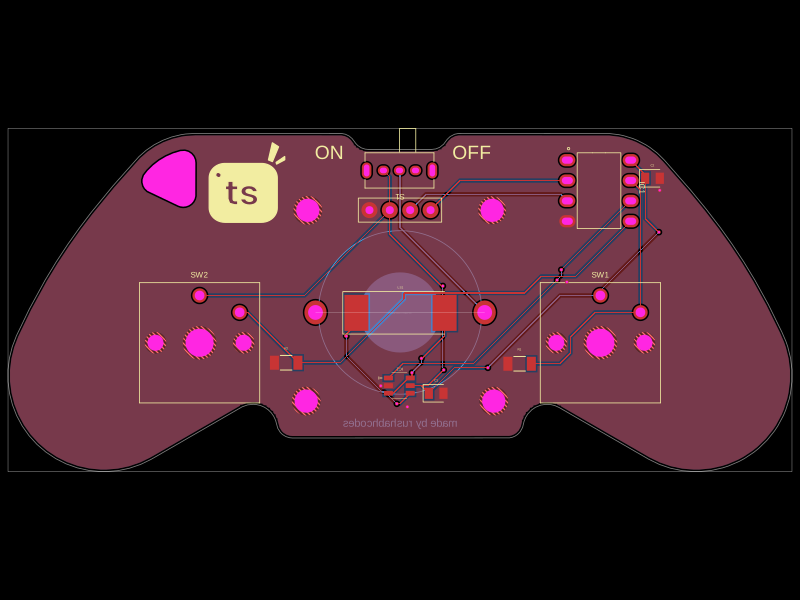 More from this authorrushabhcodes/Attiny85-Arcade-KeychainThis code defines a PCB and electronic component assembly for a compact ATtiny85-based gamepad keychain featuring power management, an OLED display, pushbutton inputs, audio piezo driver, and mechanical mounting, all mapped onto a custom PCB outline.
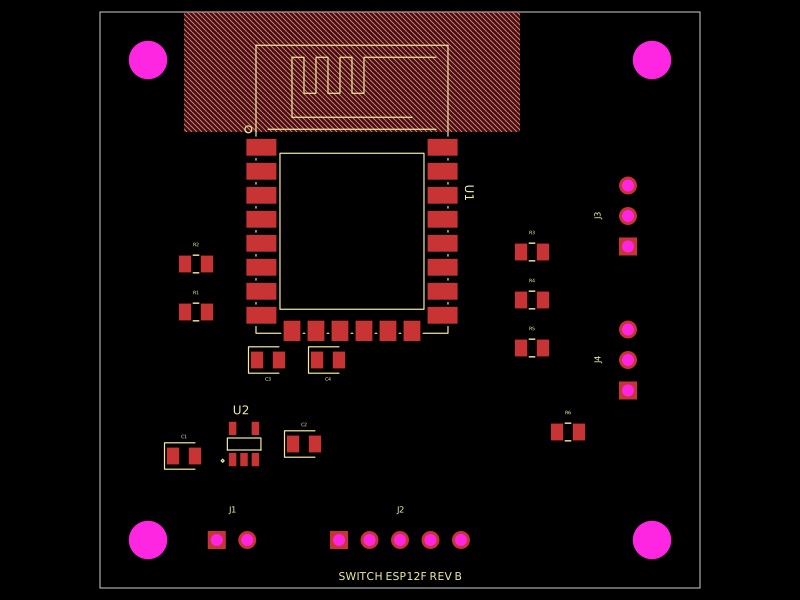 Discover something newhrithik18k/switch-pcb