rushabhcodes/fidget-counter
A tscircuit package created by rushabhcodes.
- Version
- 1.0.31
- License
- unset
- Stars
- 0
validation/check-gerber-parity.py
from pathlib import Path
import json,math,zipfile,sys,hashlib,warnings,importlib.metadata
from gerbonara import GerberFile,ExcellonFile
from gerbonara.utils import MM
from shapely.geometry import Polygon,Point,LineString,box
from shapely.affinity import rotate
from shapely.ops import unary_union
R=Path(__file__).resolve().parents[1];D=Path(sys.argv[1]if len(sys.argv)>1 else R/'dist/fabrication');c=json.load(open(D/'export.circuit.json'));z=zipfile.ZipFile(D/'gerbers.zip');out=D/'gerber-files';out.mkdir(exist_ok=True);z.extractall(out)
def primitive(p):
 n=type(p).__name__
 if n=='Circle':return Point(p.x,p.y).buffer(p.r,resolution=128)
 if n=='Rectangle':return rotate(box(p.x-p.w/2,p.y-p.h/2,p.x+p.w/2,p.y+p.h/2),p.rotation,origin=(p.x,p.y),use_radians=True)
 if n=='Line':return LineString([(p.x1,p.y1),(p.x2,p.y2)]).buffer(p.width/2,resolution=128)
 if n=='ArcPoly':
  assert all(x is None for x in p.arc_centers),'Unexpected curved region'
  return Polygon(p.outline).buffer(0)
 raise AssertionError(n)
def gerber(name):
 g=GerberFile.open(out/name);shape=Polygon();group=[];last=None
 for o in g.objects:
  for p in o.to_primitives(unit=MM):
   if last is not None and last!=p.polarity_dark:
    q=unary_union(group);shape=shape.union(q)if last else shape.difference(q);group=[]
   last=p.polarity_dark;group.append(primitive(p))
 if group:
  q=unary_union(group);shape=shape.union(q)if last else shape.difference(q)
 return shape

def pad(e):
 x,y=e['x'],e['y']
 if e['shape']=='circle':return Point(x,y).buffer(e['radius'],resolution=128)
 w,h=e['width'],e['height']
 if e['shape']=='rect':q=box(x-w/2,y-h/2,x+w/2,y+h/2)
 elif e['shape']=='pill':
  radius=min(w,h)/2
  q=LineString([(x-(w-h)/2,y),(x+(w-h)/2,y)]).buffer(radius,resolution=128)if w>=h else LineString([(x,y-(h-w)/2),(x,y+(h-w)/2)]).buffer(radius,resolution=128)
 else:raise AssertionError(e['shape'])
 return rotate(q,e.get('ccw_rotation',0),origin=(x,y))
checks={}
def parity(expected,actual,name):
 added=actual.difference(expected.buffer(.002)).area;missing=expected.difference(actual.buffer(.002)).area
 assert added<1e-7 and missing<1e-7,(name,'Fabrication artwork differs beyond2um',added,missing)
 return {'source_area_mm2':expected.area,'gerber_area_mm2':actual.area,'symmetric_difference_mm2':expected.symmetric_difference(actual).area,'unexplained_added_mm2':added,'unexplained_missing_mm2':missing}
for layer,name in [('top','F_Cu.gbr'),('bottom','B_Cu.gbr')]:
 shapes=[]
 for e in c:
  if e['type']=='pcb_smtpad'and e['layer']==layer:shapes.append(pad(e))
  if e['type']in ['pcb_via','pcb_plated_hole']and layer in e['layers']:shapes.append(Point(e['x'],e['y']).buffer(e['outer_diameter']/2,resolution=128))
  if e['type']=='pcb_copper_pour'and e['layer']==layer:
   b=e['brep_shape'];shapes.append(Polygon([(v['x'],v['y'])for v in b['outer_ring']['vertices']], [[(v['x'],v['y'])for v in h['vertices']]for h in b.get('inner_rings',[])]).buffer(0))
  if e['type']=='pcb_trace':
   for a,b in zip(e['route'],e['route'][1:]):
    if a['route_type']==b['route_type']=='wire'and a['layer']==b['layer']==layer:shapes.append(LineString([(a['x'],a['y']),(b['x'],b['y'])]).buffer(max(a['width'],b['width'])/2,resolution=128))
 expected=unary_union(shapes);actual=gerber(name);delta=expected.symmetric_difference(actual)
 checks[name]=parity(expected,actual,name)
 if layer=='top':
  for label,modified in [('removed_real_copper',actual.difference(Point(0,-17).buffer(.2))),('added_copper_in_mounting_drill',actual.union(Point(11.737973,11.737973).buffer(.5)))]:
   try:parity(expected,modified,label)
   except AssertionError:pass
   else:raise AssertionError('Gerber negative safeguard accepted '+label)
 # Mask artwork represents openings. All routing vias and GPIO interface holes
 # are covered, while the four NPTH drills and exposed SMT lands remain open.
 mask=unary_union([pad(e)for e in c if e['type']=='pcb_smtpad'and e['layer']==layer and not e.get('is_covered_with_solder_mask')]+[Point(e['x'],e['y']).buffer(e['hole_diameter']/2,resolution=128)for e in c if e['type']=='pcb_hole'])
 maskname='F_Mask.gbr'if layer=='top'else'B_Mask.gbr';checks[maskname]=parity(mask,gerber(maskname),maskname)
 paste=unary_union([pad(e)for e in c if e['type']=='pcb_solder_paste'and e['layer']==layer]);pastename='F_Paste.gbr'if layer=='top'else'B_Paste.gbr';checks[pastename]=parity(paste,gerber(pastename),pastename)
# Check the retained0.13mm via-to-foreign-pad requirement using true pill
# geometry, rather than a bounding rectangle around its rounded ends.
ports={e['pcb_port_id']:e for e in c if e['type']=='pcb_port'};source_ports={e['source_port_id']:e for e in c if e['type']=='source_port'}
minimum_via_pad=1e9;minimum_drill_pad=1e9
for via in [e for e in c if e['type']=='pcb_via']:
 for land in [e for e in c if e['type']=='pcb_smtpad'and e['layer']in via['layers']]:
  q=pad(land);distance=Point(via['x'],via['y']).distance(q)
  minimum_drill_pad=min(minimum_drill_pad,distance-via['hole_diameter']/2)
  network=source_ports.get(ports.get(land.get('pcb_port_id'),{}).get('source_port_id'),{}).get('subcircuit_connectivity_map_key')
  if network!=via.get('subcircuit_connectivity_map_key'):minimum_via_pad=min(minimum_via_pad,distance-via['outer_diameter']/2)
assert minimum_via_pad>=.13-1e-6,('Via-to-foreign-pad clearance',minimum_via_pad)
assert minimum_drill_pad>0,('Via drill intersects SMT land',minimum_drill_pad)
parsed_warnings=[]
for name in ['drill-L1-L2.drl','drill_npth.drl']:
 with warnings.catch_warnings(record=True)as ws:
  e=ExcellonFile.open(out/name)
 for w in ws:
  assert 'G90 header statement found after end of header'in str(w.message),'Unreviewed drill parsing warning'
  parsed_warnings.append('G90 absolute-position command occurs after M95; parsed positions match source')
 wanted=[(p['x'],p['y'],p['hole_diameter'])for p in c if p['type']in(['pcb_via','pcb_plated_hole']if name=='drill-L1-L2.drl'else['pcb_hole'])]
 assert len(wanted)==len(e.objects),(name,'Drill count changed')
 maximum_error=0
 for o in e.objects:
  assert type(o).__name__=='Flash'and o.unit==MM,'Unexpected slot or drill units'
  candidates=[(max(abs(o.x-x),abs(o.y-y),abs(o.aperture.diameter-d)),i)for i,(x,y,d)in enumerate(wanted)]
  error,i=min(candidates);assert error<=.00051,(name,'Drill location/size differs',error);maximum_error=max(maximum_error,error);wanted.pop(i)
 checks[name]={'holes':len(e.objects),'maximum_coordinate_or_diameter_error_mm':maximum_error}
edge=GerberFile.open(out/'Edge_Cuts.gbr');outline=next(e['outline']for e in c if e['type']=='pcb_board');assert len(edge.objects)==len(outline)==128
for i,o in enumerate(edge.objects):
 assert type(o).__name__=='Line';a=outline[i];b=outline[(i+1)%len(outline)]
 assert max(abs(o.x1-a['x']),abs(o.y1-a['y']),abs(o.x2-b['x']),abs(o.y2-b['y']))<.000002,'Board outline or closure changed'
checks['Edge_Cuts.gbr']={'closed':True,'segments':128,'diameter_mm':36.5}
paths=[Path(__file__),R/'published.circuit.json',R/'gerber-compat.mjs',R/'validation/requirements-gerber.txt']
report={'passed':True,'physical_tested':False,'parser':'gerbonara '+importlib.metadata.version('gerbonara'),'method':'Ordered dark/clear artwork primitives, independent of generator; compare complete Cu/mask/paste unions and every drill/outline segment','artwork_tolerance_mm':.002,'drill_coordinate_tolerance_mm':.00051,'layers':checks,'parser_notes':sorted(set(parsed_warnings)),'negative_checks_passed':['removed_real_copper','added_copper_in_mounting_drill'],'minimum_via_to_foreign_pad_mm':minimum_via_pad,'minimum_drill_to_any_SMT_land_mm':minimum_drill_pad,'archive_sha256':hashlib.sha256((D/'gerbers.zip').read_bytes()).hexdigest(),'source_sha256':{str(p.relative_to(R)):hashlib.sha256(p.read_bytes()).hexdigest()for p in paths}}
(R/'validation/gerber-parity-audit.json').write_text(json.dumps(report,indent=2)+'\n');print(f"PASS: independent copper/mask/paste artwork parity;{checks['drill-L1-L2.drl']['holes']} plated+4 NPTH holes and closed128-edge outline match source; two physical copper mutations rejected")
Related Packages
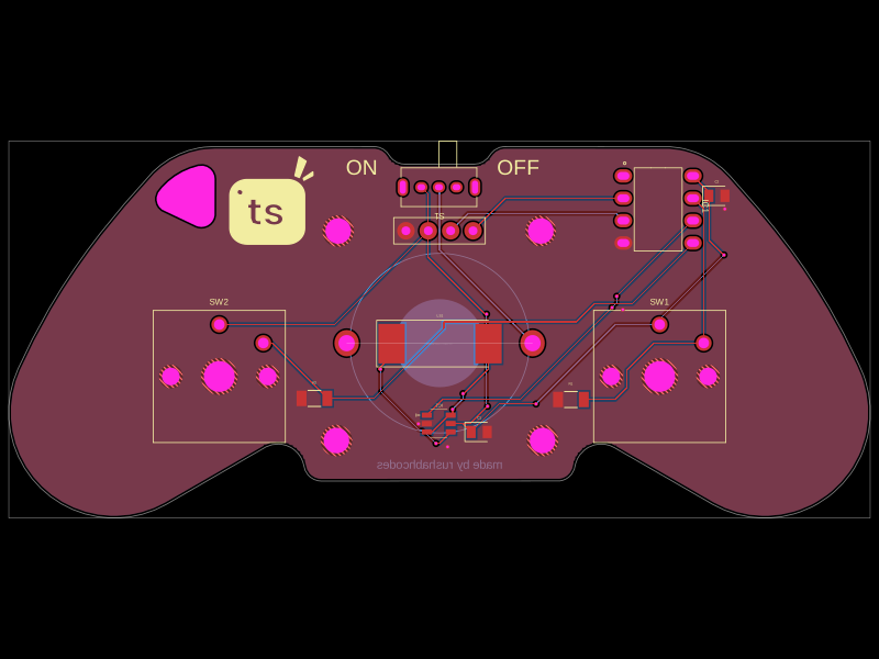 More from this authorrushabhcodes/Attiny85-Arcade-KeychainThis code defines a PCB and electronic component assembly for a compact ATtiny85-based gamepad keychain featuring power management, an OLED display, pushbutton inputs, audio piezo driver, and mechanical mounting, all mapped onto a custom PCB outline.
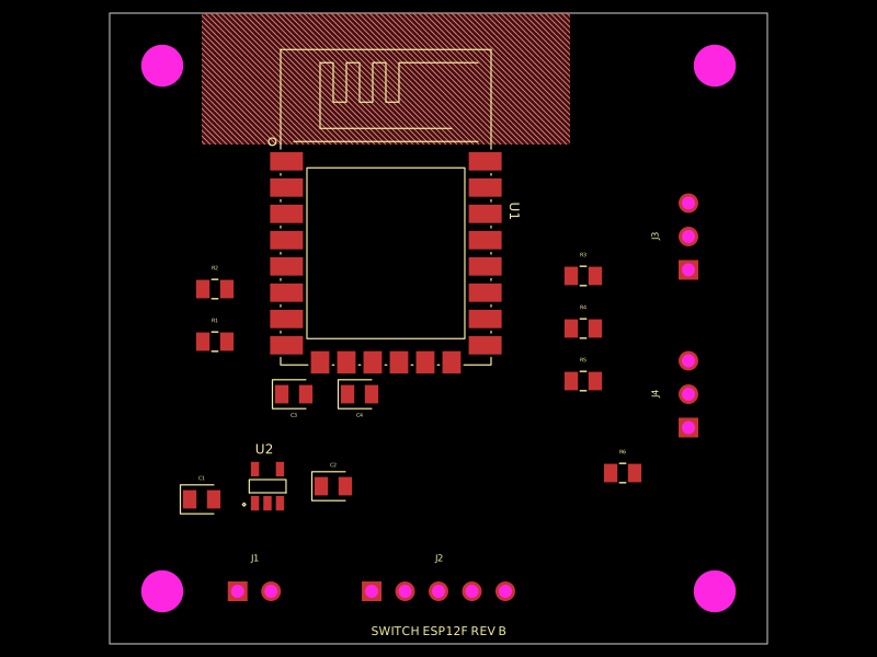 Discover something newhrithik18k/switch-pcb