rushabhcodes/fidget-counter
A tscircuit package created by rushabhcodes.
- Version
- 1.0.31
- License
- unset
- Stars
- 0
mechanical/CR2450_UPGRADE.md
# RevC CR2450 battery revision

> Historical battery/screw-joint study. The active1.0.29 compact assembly is16.4mm high; the dimensional table below records the earlier battery-only comparison. See [the compact-cap review](COMPACT_CAP_REVIEW.md). The push-fit assembly and fresh PCB routing are described in [the current pilot review](MANUFACTURING_REVIEW.md) and [fabrication review](../validation/FABRICATION_REVIEW.md).

The active design replaces CR2032 with a **3 V primary CR2450, 24.5 × 5 mm**, in the complete **MYOUNG BS-24-B4AA014 / JLCPCB C7525448** holder. It has two soldered terminals and no separate cover. The [supplier listing](https://jlcpcb.com/partdetail/MYOUNG-BS_24B4AA014/C7525448) specifies CR2450. The [manufacturer drawing](references/MYOUNG_BS-24-B4AA014_MY-CP-0246_A0.pdf), MY-CP-0246 A/0 dated 2022-03-26, is retained locally; it was obtained from [this drawing mirror](https://img.ic.ecer.com/4e/29/582cac3ab49606036a9befde434f8110.pdf).

| Dimension / inventory | Previous CR2032 | RevC CR2450 |
| --- | ---: | ---: |
| Cell | 20 × 3.2 mm | 24.5 × 5 mm |
| Panasonic reference capacity | 225 mAh | 620 mAh |
| Exterior height above phone-contact face | 17.0 mm | **17.0 mm: no increase** |
| Cap-top CAD datum | Z17.2 mm | Z17.2 mm |
| Base / maximum cap diameter | 58 / 61.6 mm | 58 / 61.6 mm |
| PCB underside / top | Z8.1 / 9.1 mm | Z10.6 / 11.6 mm |
| Encoder magnet underside / stop | Z11.4 / 12.9 mm | Z13.9 / 15.4 mm |
| Conservative JST-to-cap clearance | 3.88 mm | 1.38 mm |
| PCB drills | Four Ø3 mm at R15.2 | Four Ø2.2 mm at R16.6 |
| Rigid prints / screws / handled parts | 4 / 5 / 14 | 4 / 5 / 14 |

The [Panasonic reference](https://energy.panasonic.com/na/business/products/lithium/coin-cr-standard/models/CR2450) gives approximately 2.76 times the nominal capacity of its CR2032 reference. Product runtime has not been measured. The circuit remains non-rechargeable; LIR2450 is not a substitute, and there is no charger.

## PCB and enclosure changes

The Ø36.5 × 1 mm PCB keeps its outline and the other 27 fitted components at their previous XY positions. BT1 is centered, with the original supplier lands: two 3.3999932 × 3.5999928 mm pads at X±15.550007 mm. On the bottom layer, pin 1 is at −X and connects to VBAT; pin 2 is at +X and connects to GND. Two battery branch traces change. Two tented Ø0.3/0.55 mm through vias carry a short ground bridge over the retained positive route. Other trace/via/pad geometry, pin functions, signal connectivity, layers and route constraints remain guarded against commit `346fade`. Ground pours are regenerated around the changed lands, drills and keepouts; a separate BREP-area comparison rejects any copper difference outside those specified regions and includes three failing copper/layer/mask safeguards.

The board and encoder magnet rise 2.5 mm together, preserving their relative sensing gap (nominally 1.8 mm). The base has four narrower, outward-moved posts with 0.8 mm nominal pilot walls and no locating collars. The two nylon screws locate and retain the board through close-clearance holes. The nominal PCB hole-to-edge web is 0.55 mm. Three bearing webs move outward and have smaller upper heads to clear the holder. All 11 cap styles have a higher encoder pocket/stop. Bearing, inner nut, outer retainer, cap screws, ring seat and exterior envelope remain unchanged.

The holder body is 7.6 mm high, but its drawing shows an **8.6 mm loaded outline**. The enclosure allows the full loaded height, leaving 0.5 mm nominal clearance between the cell and the 1.5 mm base floor. Do not size the cavity using the empty-holder height alone.

## Model and courtyard control

The exact imported TSX footprint, STEP and OBJ remain unchanged. The application wrapper aligns the CAD model's circular housing axis to the land-pattern center instead of its asymmetric bounding-box center; its mounting-plane datum stays Z−0.9 mm.

The compiler approximates body-outline/drill overlap using bounding boxes. Native courtyards therefore cover the solder terminals, while a separate mandatory check uses the complete supplier-model XY projection, expanded by 0.20 mm, for body clearance against all four drills and posts. Continuous insertion uses proven height-sliced projection prisms, preserving the fact that solder tabs start above the bearing webs. A full component AABB would invent solid material in the empty corners of this round holder. Real source-model intersections still fail validation.

The supplier STEP depicts free-state spring contacts intruding into the nominal cell volume. The cell check permits only the two drawing-identified contact regions, with a strict volume bound; any other intersection fails. This is **not** a simulation of loaded contact force or proof of physical seating. The old C964813 cover conflict is avoided by selecting a different holder; that supplier model has not been edited to manufacture clearance.

The holder's insulating LCP housing enters part of the antenna's XY reserve. Its drawing-based conductor strip and the cell remain outside that copper reserve. This does not qualify RF performance: the larger cell and added dielectric loading require populated BLE/RF measurement and antenna matching in the final assembly.

## Verification and release limits

Run the README rebuild sequence. The active evidence includes `validation/cr2450-circuit-audit.json`, `cr2450-cad-audit.json`, `cr2450-copper-audit.json`, `cr2450-holder-audit.json`, `cr2450-display-audit.json`, `pcb-insertion-audit.json` and `print-readiness.json`. Electrical regression tests deliberately reject unrelated component movement, copper width/layer changes, modified battery routes, wrong drills, changed connectivity and altered added-via layers. The router still rejects any unrecognized terminal, net, obstacle, copper or design-rule change.

The printed pilot still needs a physical cell/holder sample, polarity and loaded-contact/retention checks, printed fits/support removal, PCB edge/retention testing, thread and screw strength, adhesive retention, magnetic sensing, RF/firmware and runtime tests. No assembly time, runtime or manufacturing qualification is claimed. Do not mix RevC PCB/base/cap files with the older CR2032 prints or BOM.
Related Packages
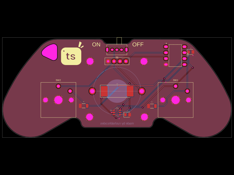 More from this authorrushabhcodes/Attiny85-Arcade-KeychainThis code defines a PCB and electronic component assembly for a compact ATtiny85-based gamepad keychain featuring power management, an OLED display, pushbutton inputs, audio piezo driver, and mechanical mounting, all mapped onto a custom PCB outline.
 Discover something newhrithik18k/switch-pcb