rushabhcodes/Attiny85-Arcade-Keychain
This code defines the hardware layout of an ATtiny85-based arcade-style gamepad keychain, featuring a custom PCB with power management, an OLED display, push buttons, an oscillator, a piezo transducer driven via a inverter, mechanical mounting holes, and silkscreen graphics, all modeled with detailed component footprints and electrical traces.
- Version
- 1.0.4
- License
- unset
- Stars
- 2
index.circuit.tsx
PCB
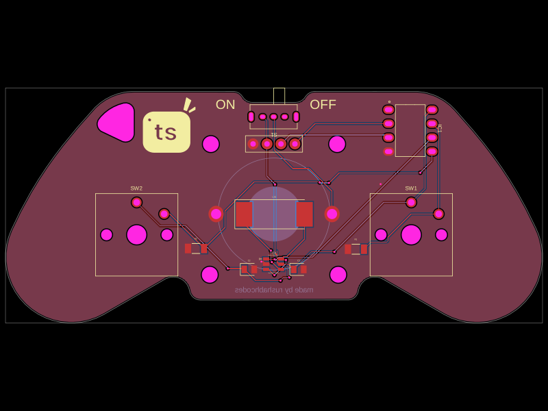
Schematic

/**
 * ATtiny85 Arcade — "Armour Grade" gamepad keychain, rev 1.1
 *
 * A tscircuit recreation of the reference design
 * (Attiny_Arcader_game_rev_1.1 schematic + Attiny-Arcade_Keychain_2.0 Gerbers).
 *
 * How it works
 *   A CR2032 on the underside feeds the board through the SK-12D02VG3 slide switch.
 *   The ATtiny85 talks software-I2C to a 4-pin 0.96" OLED module on PB3/PB4,
 *   reads two Kailh Choc keyswitches on PB0/PB2 (10k pull-downs), and drives a
 *   Murata piezo from PB1 through an SN74LVC2G04 dual inverter wired as a
 *   bridge-tied load — 1Y and 2Y swing in antiphase, so the transducer sees
 *   ~2x the rail.
 *   PB5/RESET is deliberately left floating so the part stays ISP-programmable.
 *
 * Every PCB coordinate is lifted from the reference Gerbers and re-referenced
 * to the board centre at (176.848 mm, -59.9235 mm) in the original artwork.
 */
import type { ChipProps } from "tscircuit";
import {
  BOARD_OUTLINE,
  KEYCHAIN_CUTOUT,
  KEYCHAIN_CUTOUT_CENTER,
} from "./board-outline";
import { ATTINY85_20PU } from "./imports/ATTINY85_20PU";
import { PKLCS1212E2000_R1 } from "./imports/PKLCS1212E2000_R1";
import { SN74LVC2G04DBVR } from "./imports/SN74LVC2G04DBVR";
import { SK_12D02VG3 } from "./imports/SK_12D02VG3";
import { CPG135001D03 } from "./imports/CPG135001D03";
import { CoinCellHolder3003 } from "./imports/CoinCellHolder3003";
import { OledDisplay } from "./imports/OledDisplay";

const tscircuitLogoSvg = `data:image/svg+xml,${encodeURIComponent(`
<svg
   viewBox="0 0 92 101"
   version="1.1"
   id="svg5"
   sodipodi:docname="tscircuit-logo.svg"
   inkscape:version="1.4.4 (dcaf3e7d9e, 2026-05-05)"
   xmlns:inkscape="http://www.inkscape.org/namespaces/inkscape"
   xmlns:sodipodi="http://sodipodi.sourceforge.net/DTD/sodipodi-0.dtd"
   xmlns="http://www.w3.org/2000/svg"
   xmlns:svg="http://www.w3.org/2000/svg">
  <defs
     id="defs5" />
  <sodipodi:namedview
     id="namedview5"
     pagecolor="#ffffff"
     bordercolor="#999999"
     borderopacity="1"
     inkscape:showpageshadow="2"
     inkscape:pageopacity="0"
     inkscape:pagecheckerboard="0"
     inkscape:deskcolor="#d1d1d1"
     inkscape:zoom="5.9018913"
     inkscape:cx="56.422592"
     inkscape:cy="51.932505"
     inkscape:window-width="1920"
     inkscape:window-height="1052"
     inkscape:window-x="0"
     inkscape:window-y="0"
     inkscape:window-maximized="1"
     inkscape:current-layer="svg5" />
  <path
     d="m 19.872307,100.852 -2.349,-0.154 -2.31,-0.459 -2.229,-0.757 -2.112,-1.042 -1.9580002,-1.308 -1.77,-1.552 -1.552,-1.77 -1.308,-1.958 -1.042,-2.112 -0.757,-2.229 -0.459,-2.31 -0.154,-2.349 v -38 l 0.154,-2.349 0.459,-2.31 0.757,-2.229 1.042,-2.112 1.308,-1.958 1.552,-1.77 1.77,-1.552 1.9580002,-1.308 2.112,-1.042 2.229,-0.757 2.31,-0.459 2.349,-0.154 h 42 l 2.349,0.154 2.31,0.459 2.229,0.757 2.112,1.042 1.958,1.308 1.77,1.552 1.552,1.77 1.308,1.958 1.042,2.112 0.757,2.229 0.459,2.31 0.154,2.349 v 38 l -0.154,2.349 -0.459,2.31 -0.757,2.229 -1.042,2.112 -1.308,1.958 -1.552,1.77 -1.77,1.552 -1.958,1.308 -2.112,1.042 -2.229,0.757 -2.31,0.459 -2.349,0.154 z"
     fill="#000000"
     id="path1" />
  <path
     d="m 12.372307,37.852 c 2.6943,0 4.3782,2.9167 3.0311,5.25 -0.6252,1.0829 -1.7807,1.75 -3.0311,1.75 -2.6943002,0 -4.3782002,-2.9167 -3.0311002,-5.25 0.6252,-1.0829 1.7807002,-1.75 3.0311002,-1.75 z"
     fill="#ffffff"
     id="path2" />
  <path
     d="m 29.297007,59.975 v 11.524 c 0,0.8026 0.1864,1.3903 0.559,1.763 0.4014,0.344 1.0607,0.516 1.978,0.516 h 2.795 v 5.074 h -3.784 c -5.074,0 -7.611,-2.4654 -7.611,-7.396 V 59.975 h -2.838 V 55.03 h 2.838 v -5.891 h 6.063 v 5.891 h 5.332 v 4.945 z m 18.7779,19.264 c -1.9493,0 -3.698,-0.344 -5.246,-1.032 -1.548,-0.7167 -2.7806,-1.677 -3.698,-2.881 -0.8886,-1.204 -1.376,-2.537 -1.462,-3.999 h 6.063 c 0.1147,0.9173 0.559,1.677 1.333,2.279 0.8027,0.602 1.7917,0.903 2.967,0.903 1.1467,0 2.0354,-0.2294 2.666,-0.688 0.6594,-0.4587 0.989,-1.0464 0.989,-1.763 0,-0.774 -0.4013,-1.3474 -1.204,-1.72 -0.774,-0.4014 -2.021,-0.8314 -3.741,-1.29 -1.7773,-0.43 -3.2393,-0.8744 -4.386,-1.333 -1.118,-0.4587 -2.0926,-1.161 -2.924,-2.107 -0.8026,-0.946 -1.204,-2.2217 -1.204,-3.827 0,-1.3187 0.3727,-2.5227 1.118,-3.612 0.774,-1.0894 1.8634,-1.9494 3.268,-2.58 1.4334,-0.6307 3.1104,-0.946 5.031,-0.946 2.838,0 5.1027,0.7166 6.794,2.15 1.6914,1.4046 2.623,3.311 2.795,5.719 h -5.762 c -0.086,-0.946 -0.4873,-1.6914 -1.204,-2.236 -0.688,-0.5734 -1.6196,-0.86 -2.795,-0.86 -1.0893,0 -1.935,0.2006 -2.537,0.602 -0.5733,0.4013 -0.86,0.9603 -0.86,1.677 0,0.8026 0.4014,1.419 1.204,1.849 0.8027,0.4013 2.0497,0.817 3.741,1.247 1.72,0.43 3.139,0.8743 4.257,1.333 1.118,0.4586 2.0784,1.1753 2.881,2.15 0.8314,0.946 1.2614,2.2073 1.29,3.784 0,1.376 -0.387,2.6086 -1.161,3.698 -0.7453,1.0893 -1.8346,1.9493 -3.268,2.58 -1.4046,0.602 -3.053,0.903 -4.945,0.903 z"
     fill="#ffffff"
     id="path3" />
  <path
     d="m 69.872307,22.352 4.5,2 7,-18.5 -7,-5 z"
     fill="#000000"
     stroke="#000000"
     id="path4" />
  <path
     d="m 78.658007,25.4493 0.5267,2.0892 9.3097,-5.3919 -0.0773,-4.0052 z"
     fill="#000000"
     stroke="#000000"
     id="path5" />
</svg>
  `)}`;

/**
 * The registry part ships generic pin1..pin8 labels. Re-label them so the
 * traces below can talk in PBn terms, and re-type the component so those
 * names are what the compiler checks the selectors against.
 */
const ATTINY85_PIN_LABELS = {
  pin1: ["PB5", "RESET"],
  pin2: ["PB3", "XTAL1"],
  pin3: ["PB4", "XTAL2"],
  pin4: "GND",
  pin5: ["PB0", "MOSI", "AREF"],
  pin6: ["PB1", "MISO", "OC0B"],
  pin7: ["PB2", "SCK", "INT0"],
  pin8: "VCC",
} as const;

const Attiny85 = ATTINY85_20PU as (
  props: ChipProps<typeof ATTINY85_PIN_LABELS>,
) => ReturnType<typeof ATTINY85_20PU>;

export default () => (
  <board
    outline={BOARD_OUTLINE}
    layers={2}
    thickness="1.6mm"
    title="ATtiny85 Arcade Keychain"
    minViaHoleDiameter="0.3mm"
    minViaPadDiameter="0.45mm"
  >
    <schematicsection name="Power" displayName="Power" />
    <schematicsection name="MCU" displayName="ATtiny85" />
    <schematicsection name="Display" displayName="OLED" />
    <schematicsection name="Buttons" displayName="Buttons" />
    <schematicsection name="Audio" displayName="Audio" />

    {/* ---------------- Power ---------------- */}
    <CoinCellHolder3003
      name="BT1"
      schSectionName="Power"
      schX={-20}
      schY={5}
      layer="bottom"
      pcbX={0.0122}
      pcbY={-1.2397}
      doNotPlace
    />
    <SK_12D02VG3
      name="S1"
      schSectionName="Power"
      schX={-24}
      schY={5}
      pcbX={-0.064}
      pcbY={16.4735}
      pcbRotation={180}
    />
    <capacitor
      name="C1"
      capacitance="100nF"
      footprint="0805"
      schSectionName="Power"
      schX={-24}
      schY={-1}
      schOrientation="vertical"
      pcbX={4.508}
      pcbY={-11.3235}
    />
    <capacitor
      name="C2"
      capacitance="100nF"
      footprint="0805"
      schSectionName="Power"
      schX={-20}
      schY={-1}
      schOrientation="vertical"
      pcbX={-4.508}
      pcbY={-11.3235}
      />

    {/* ---------------- MCU ---------------- */}
    <Attiny85
      name="IC1"
      pinLabels={ATTINY85_PIN_LABELS}
      schPinArrangement={{
        leftSide: {
          pins: ["PB5", "PB3", "PB4", "GND"],
          direction: "top-to-bottom",
        },
        rightSide: {
          pins: ["VCC", "PB2", "PB1", "PB0"],
          direction: "top-to-bottom",
        },
      }}
      schSectionName="MCU"
      schX={-3}
      schY={2}
      pcbX={24.828}
      pcbY={13.9495}
      pcbRotation={-90}
    />

    {/* ---------------- Display ---------------- */}
    <OledDisplay
      name="U1"
      schSectionName="Display"
      schX={-11}
      schY={2}
      pcbX={0}
      pcbY={11.5266}
    />

    {/* ---------------- Buttons ---------------- */}
    <resistor
      name="R1"
      resistance="10k"
      footprint="1206"
      schSectionName="Buttons"
      schX={6}
      schY={5}
      schRotation={90}
      pcbX={14.922}
      pcbY={-7.6405}
    />
    <CPG135001D03
      name="SW1"
      schSectionName="Buttons"
      schX={10}
      schY={7}
      pcbX={25}
      pcbY={-2.5}
    />
    <resistor
      name="R2"
      resistance="10k"
      footprint="1206"
      schSectionName="Buttons"
      schX={6}
      schY={-1}
      schRotation={90}
      pcbX={-14.2}
      pcbY={-7.5135}
    />
    <CPG135001D03
      name="SW2"
      schSectionName="Buttons"
      schX={10}
      schY={1}
      pcbX={-25}
      pcbY={-2.5}
    />

    {/* ---------------- Audio ---------------- */}
    <SN74LVC2G04DBVR
      name="IC2"
      schPinArrangement={{
        leftSide: { pins: ["VCC", "1A", "2A"], direction: "top-to-bottom" },
        rightSide: { pins: ["GND", "1Y", "2Y"], direction: "top-to-bottom" },
      }}
      schSectionName="Audio"
      schX={-6.06}
      schY={-9}
      pcbX={-0.084}
      pcbY={-10.3685}
      pcbRotation={180}
    />
    {/* Murata PKLCS1212E2000 in place of the reference CPT-1203-78-SMT-TR:
        same 12 mm body sitting over the battery holder, pin 1 to the left. */}
    <PKLCS1212E2000_R1
      name="LS1"
      schSectionName="Audio"
      schX={-0.21}
      schY={-10.27}
      pcbX={0.063}
      pcbY={-1.2905}
    />

    {/* ---------------- Mechanical ---------------- */}
    {/* Mounting holes are already treated as autorouter obstacles. */}
    <hole name="MH1" diameter="2.9mm" pcbX={-11.5} pcbY={11.5} />
    <hole name="MH2" diameter="2.9mm" pcbX={11.5} pcbY={11.5} />
    <hole name="MH3" diameter="2.9mm" pcbX={-11.7} pcbY={-12.3} />
    <hole name="MH4" diameter="2.9mm" pcbX={11.7} pcbY={-12.3} />
    <cutout
      shape="polygon"
      points={KEYCHAIN_CUTOUT}
      pcbX={KEYCHAIN_CUTOUT_CENTER.x}
      pcbY={KEYCHAIN_CUTOUT_CENTER.y}
    />

    {/* ---------------- Silkscreen ---------------- */}
    <silkscreentext text="ON" fontSize={2.4} pcbX={-8.9} pcbY={18.7} />
    <silkscreentext text="OFF" fontSize={2.4} pcbX={8.9} pcbY={18.7} />
    <silkscreengraphic
      imageUrl={tscircuitLogoSvg}
      width="10mm"
      height="10mm"
      pcbX={-19}
      pcbY={15}
    />
    <silkscreentext
      text="made by rushabhcodes"
      layer={"bottom"}
      fontSize={1.4}
      pcbX={0}
      pcbY={-15}
    />

    {/* ---------------- Power distribution ---------------- */}
    <trace from=".BT1 > .plus" to=".S1 > .COM" />
    <trace from=".BT1 > .minus" to="net.GND" />
    <trace from=".S1 > .NC" to="net.V3" />

    <trace from=".IC1 > .VCC" to="net.V3" />
    <trace from=".IC1 > .GND" to="net.GND" />
    <trace from=".IC2 > .VCC" to="net.V3" />
    <trace from=".IC2 > .GND" to="net.GND" />
    <trace from=".U1 > .VDD" to="net.V3" />
    <trace from=".U1 > .GND" to="net.GND" />
    <trace from=".C1 > .pin1" to="net.V3" />
    <trace from=".C1 > .pin2" to="net.GND" />
    <trace from=".C2 > .pin1" to="net.V3" />
    <trace from=".C2 > .pin2" to="net.GND" />

    {/* ---------------- OLED (software I2C) ---------------- */}
    <trace from=".IC1 > .PB3" to=".U1 > .SDA" />
    <trace from=".IC1 > .PB4" to=".U1 > .SCK" />

    {/* ---------------- Buttons: switch to +3V, 10k pull-down ---------------- */}
    <trace from=".SW1 > .pin1" to="net.V3" />
    <trace from=".SW1 > .pin2" to=".IC1 > .PB2" />
    <trace from=".R1 > .pin2" to=".IC1 > .PB2" />
    <trace from=".R1 > .pin1" to="net.GND" />

    <trace from=".SW2 > .pin1" to="net.V3" />
    <trace from=".SW2 > .pin2" to=".IC1 > .PB0" />
    <trace from=".R2 > .pin2" to=".IC1 > .PB0" />
    <trace from=".R2 > .pin1" to="net.GND" />

    {/* ---------------- Audio: bridge-tied piezo drive ---------------- */}
    <trace from=".IC1 > .PB1" to=".IC2 > .1A" />
    <trace from=".IC2 > .1Y" to=".IC2 > .2A" />
    <trace from=".IC2 > .1Y" to=".LS1 > .pin2" />
    <trace from=".IC2 > .2Y" to=".LS1 > .pin1" />

    {/* Ground pour on both layers, matching the reference artwork. */}
    <copperpour connectsTo="net.GND" layer="top" />
    <copperpour connectsTo="net.GND" layer="bottom" />
  </board>
);