pixalynx/esp32-gps-cellular-tracker
This code defines a hardware layout comprising a Wi-Fi-enabled ESP32 module, GPS module, cellular GSM module, battery management components (including charger, protection circuits, and voltage regulators), USB-C connector, SIM card holder, RF components, and supporting passive components for a comprehensive GPS+Cellular tracker device.
- Version
- 1.1.0
- License
- unset
- Stars
- 0
index.circuit.tsx
PCB
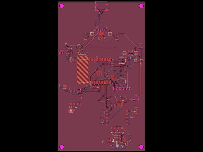
Schematic

import { ESP32_WROOM_32E_N4 } from "./imports/ESP32_WROOM_32E_N4"
import { ATGM336H_5N31 } from "./imports/ATGM336H_5N31"
import { SIM800C } from "./imports/SIM800C"
import { TP4056_42_ESOP8 } from "./imports/TP4056_42_ESOP8"
import { DW01A } from "./imports/DW01A"
import { FS8205A } from "./imports/FS8205A"
import { AP2112K_3_3TRG1 } from "./imports/AP2112K_3_3TRG1"
import { BWU_FL_IPEX1 } from "./imports/BWU_FL_IPEX1"
import { SMN_304 } from "./imports/SMN_304"
import { B2B_PH_K_S_LF__SN_ as JST_PH2 } from "./imports/B2B_PH_K_S_LF__SN_"
import { MSK12C02 } from "./imports/MSK12C02"
import { ERR1AM102F12OT } from "./imports/ERR1AM102F12OT"
import { TS_1187A_B_A_B } from "./imports/TS_1187A_B_A_B"
import { AO3401A } from "./imports/AO3401A"
import { SS14L } from "./imports/SS14L"
import { TYPE_C_16PIN_2MD_073 } from "./imports/TYPE_C_16PIN_2MD_073"
// Schematic sections laid out on a grid, spaced so each section's internal
// offsets don't collide with its neighbors.
const SEC = {
Usb: { x: 0, y: 34 },
Charger: { x: 0, y: 17 },
Protection: { x: -20, y: 17 },
Regulator: { x: 20, y: 17 },
Mcu: { x: 0, y: 0 },
BootReset: { x: 20, y: 0 },
Gps: { x: -20, y: -17 },
Cellular: { x: 0, y: -17 },
SimCard: { x: 20, y: -17 },
}
// ESP32-WROOM-32E's own printed PCB antenna sits in the ~6.3mm-wide strip at
// the narrow end of the module opposite the two 14-pad rows (visible in the
// imported footprint as the tall silkscreen sliver from x=-16.76 to -10.48mm,
// module-local coordinates). No copper is allowed there on either layer or
// it detunes the antenna. The keepout extends ~2.5mm past the antenna on its
// left and top sides and 1mm below it (the GPS UART traces enter the ESP32's
// bottom pad row from that corner, and the router clipped a wider margin
// there); its right edge stops short of the first pad column (pins 1/38 at
// x=-9.29).
// Espressif's guideline is stricter still -- antenna at the board edge with
// nothing metallic nearby -- so expect reduced Wi-Fi/BT range compared to a
// dev kit. The tracker's primary link is the GSM modem, so this is a
// tradeoff, not a blocker.
const ESP32_LOCAL_ANTENNA_OFFSET = { x: -14.79, y: 0.8, width: 9.22, height: 21.6 }
// Bottom-layer "via fence" under every ESP32 perimeter pad (module-local
// coordinates, pads are 0.95 x 2.1mm on a 1.27mm pitch). Each strip is
// 0.65mm across and runs 0.55mm past both ends of its pad. The 0.62mm lanes
// left between neighbours still pass a 0.15mm trace at the router's 0.2mm
// obstacle margin, but a 0.4mm via cannot fit in a lane or sit against a pad
// end, which is exactly where the local router kept parking layer changes
// (0-0.05mm from the neighbouring pad). Row-end pads get the strip widened
// on their outer side for the same reason. The ESP32 pads are top-layer
// only, so these bottom-layer strips never touch real copper.
const ESP32_VIA_FENCE_RECTS = (() => {
const rects: { x: number; y: number; w: number; h: number }[] = []
const rowXs = Array.from({ length: 14 }, (_, i) => -9.29 + i * 1.27)
for (const rowY of [-9.0, 9.0]) {
rowXs.forEach((x, i) => {
const end = i === 0 ? -1 : i === 13 ? 1 : 0
rects.push({ x: x + end * 0.225, y: rowY, w: 0.65 + Math.abs(end) * 0.45, h: 3.2 })
})
}
// Right column: only pins 15, 16, 23, 24 still have pads (NC pads removed).
for (const y of [-5.715, -4.445, 4.445, 5.715]) {
const end = y === -5.715 ? -1 : y === 5.715 ? 1 : 0
rects.push({ x: 8.715, y: y + end * 0.225, w: 3.2, h: 0.65 + Math.abs(end) * 0.45 })
}
return rects
})()
export default () => {
const mcuPos = { x: 0, y: 4.143 }
const antennaKeepout = {
pcbX: mcuPos.x + ESP32_LOCAL_ANTENNA_OFFSET.x,
pcbY: mcuPos.y + ESP32_LOCAL_ANTENNA_OFFSET.y,
width: ESP32_LOCAL_ANTENNA_OFFSET.width,
height: ESP32_LOCAL_ANTENNA_OFFSET.height,
}
return (
<board
width="68mm"
height="116mm"
layers={2}
title="ESP32 GPS + Cellular Tracker"
// 0.2/0.4mm vias clear JLCPCB's 2-layer minimum (0.15/0.25mm). The
// DRC floor below is JLCPCB's published 0.10mm (4 mil) trace/space
// for 1oz 2-layer; the <autoroutingphase> asks the router for more
// than that because it lands short of whatever margin it is given in
// dense spots. (autorouter.traceClearance is not read by the local
// router, so it is not used here.)
pcbStyle={{ viaHoleDiameter: "0.2mm", viaPadDiameter: "0.4mm" }}
minTraceToPadEdgeClearance="0.1mm"
minViaEdgeToPadEdgeClearance="0.1mm"
>
<autoroutingphase
minTraceToPadEdgeClearance="0.2mm"
minViaEdgeToPadEdgeClearance="0.25mm"
/>
{/* M3 mounting holes, one per corner */}
<hole name="H1" diameter="3.2mm" pcbX={-31} pcbY={55} />
<hole name="H2" diameter="3.2mm" pcbX={31} pcbY={55} />
<hole name="H3" diameter="3.2mm" pcbX={-31} pcbY={-55} />
<hole name="H4" diameter="3.2mm" pcbX={31} pcbY={-55} />
<net name="GND" isGroundNet />
<net name="USB5V" isPowerNet />
<net name="VBAT" isPowerNet />
<net name="VSYS" isPowerNet />
<net name="MCU_PWR" isPowerNet />
<net name="V3V3" isPowerNet />
<schematicsection name="Usb" displayName="USB-C Charging Input" />
<schematicsection name="Charger" displayName="TP4056 Li-ion Charger" />
<schematicsection
name="Protection"
displayName="Battery + Protection (DW01A/FS8205A)"
/>
<schematicsection name="Regulator" displayName="3.3V Regulation" />
<schematicsection name="Mcu" displayName="ESP32-WROOM-32E" />
<schematicsection
name="BootReset"
displayName="Boot / Reset / UART Header"
/>
<schematicsection name="Gps" displayName="GPS (ATGM336H, UART)" />
<schematicsection
name="Cellular"
displayName="SIM800C GSM/GPRS + SIM Card"
/>
<schematicsection name="SimCard" displayName="Nano-SIM Holder" />
{/* ============================ USB-C Charging Input ============================
Charge-only port: no data lines used. CC1/CC2 pulldowns are required
so a USB-C source enumerates this as a sink and actually supplies 5V. */}
{/* Footprint is spelled out in the import (see the note there); it is
the same C2765186 geometry the parts engine fetches, verified
against the EasyEDA footprint: top-mount SMD, 7.35mm deep body,
not a mid-mount. Receptacle body extends 7.35mm from the pad row
toward the board edge (y=58); this position puts its mating face
~0.6mm past the edge so a plug's overmold clears the PCB, while
the shell slots and peg holes stay >1mm inside the edge. */}
<TYPE_C_16PIN_2MD_073
name="J1"
pcbX={0}
pcbY={53.4}
pcbRotation={180}
schSectionName="Usb"
schX={SEC.Usb.x}
schY={SEC.Usb.y}
/>
<resistor
name="R1"
resistance="5.1k"
footprint="0402"
pcbX={-4.359}
pcbY={38.114}
schSectionName="Usb"
schX={SEC.Usb.x - 4}
schY={SEC.Usb.y - 4}
/>
<resistor
name="R2"
resistance="5.1k"
footprint="0402"
pcbX={4.359}
pcbY={38.114}
schSectionName="Usb"
schX={SEC.Usb.x + 4}
schY={SEC.Usb.y - 4}
/>
<trace from="J1.VBUS1" to="net.USB5V" thickness="0.4mm" />
<trace from="J1.VBUS2" to="net.USB5V" thickness="0.4mm" />
<trace from="J1.GND1" to="net.GND" />
<trace from="J1.GND2" to="net.GND" />
<trace from="J1.SHELL1" to="net.GND" />
<trace from="J1.SHELL2" to="net.GND" />
<trace from="J1.SHELL3" to="net.GND" />
<trace from="J1.SHELL4" to="net.GND" />
<trace from="J1.CC1" to="R1.pin1" />
<trace from="R1.pin2" to="net.GND" />
<trace from="J1.CC2" to="R2.pin1" />
<trace from="R2.pin2" to="net.GND" />
{/* ============================ TP4056 Li-ion Charger ============================ */}
<TP4056_42_ESOP8
name="U1"
pcbX={0}
pcbY={33.142}
schSectionName="Charger"
schX={SEC.Charger.x}
schY={SEC.Charger.y + 0.78}
/>
{/* maxDecouplingTraceLength on the caps below is set above the
physical cap-to-pin distance: the checker measures every routed
trace touching the cap, including the net continuing onward from
it. Without an explicit value tscircuit assumes 1mm for any
power-to-ground cap and silently skips autorouting when that is
not achievable. */}
<capacitor
name="C1"
maxDecouplingTraceLength="30mm"
capacitance="10uF"
footprint="0805"
schOrientation="vertical"
pcbX={-6.974}
pcbY={33.142}
schSectionName="Charger"
schX={SEC.Charger.x - 5}
schY={SEC.Charger.y}
/>
<capacitor
name="C2"
maxDecouplingTraceLength="30mm"
capacitance="10uF"
footprint="0805"
schOrientation="vertical"
pcbX={6.974}
pcbY={33.142}
schSectionName="Charger"
schX={SEC.Charger.x + 5}
schY={SEC.Charger.y}
/>
{/* R3 sets charge current: Ibat[mA] = 1200 / R3[kOhm] -> ~500mA, a
conservative default for small (500-1200mAh) tracker battery packs. */}
<resistor
name="R3"
resistance="2.4k"
footprint="0402"
pcbX={0}
pcbY={28.171}
schSectionName="Charger"
schX={SEC.Charger.x}
schY={SEC.Charger.y - 4}
/>
<led
name="LED1"
color="red"
footprint="0603"
schRotation={90}
pcbX={-12.205}
pcbY={29.829}
schSectionName="Charger"
schX={SEC.Charger.x - 9}
schY={SEC.Charger.y - 1}
/>
<resistor
name="R4"
resistance="330"
footprint="0402"
schOrientation="vertical"
pcbX={-12.205}
pcbY={33.142}
schSectionName="Charger"
schX={SEC.Charger.x - 9}
schY={SEC.Charger.y - 4}
/>
<led
name="LED2"
color="green"
footprint="0603"
schRotation={90}
pcbX={12.205}
pcbY={29.829}
schSectionName="Charger"
schX={SEC.Charger.x + 9}
schY={SEC.Charger.y - 1}
/>
<resistor
name="R5"
resistance="330"
footprint="0402"
schOrientation="vertical"
pcbX={12.205}
pcbY={33.142}
schSectionName="Charger"
schX={SEC.Charger.x + 9}
schY={SEC.Charger.y - 4}
/>
<trace from="net.USB5V" to="U1.VCC" thickness="0.4mm" />
<trace from="U1.GND" to="net.GND" />
<trace from="U1.CE" to="net.USB5V" />
<trace from="U1.TEMP" to="net.GND" />
<trace from="U1.EP" to="net.GND" />
<trace from="U1.BAT" to="net.VBAT" thickness="0.6mm" />
<trace from="U1.PROG" to="R3.pin1" />
<trace from="R3.pin2" to="net.GND" />
<trace from="C1.pin1" to="net.USB5V" thickness="0.4mm" />
<trace from="C1.pin2" to="net.GND" />
<trace from="C2.pin1" to="net.VBAT" thickness="0.4mm" />
<trace from="C2.pin2" to="net.GND" />
<trace from="U1.N_CHRG" to="LED1.cathode" />
<trace from="LED1.anode" to="R4.pin1" />
<trace from="R4.pin2" to="net.USB5V" />
<trace from="U1.N_STDBY" to="LED2.cathode" />
<trace from="LED2.anode" to="R5.pin1" />
<trace from="R5.pin2" to="net.USB5V" />
{/* ============================ Battery + Protection ============================
Standard 1S Li-ion "charge + discharge protection" topology from the
DW01A datasheet reference circuit. FS8205A is a COMMON-DRAIN dual
N-FET: its two drains are joined inside the package, so the two
sources are the outer terminals -- S1 to the raw cell negative
(B-), S2 to the protected system ground (P-). Both charge and
discharge current pass through the pair. G1 (=OD) blocks discharge
on under-voltage/over-current; G2 (=OC) blocks charge on
over-voltage. Only the raw cell negative and the DW01A's own supply
node sit "before" the FETs; everything else, including the
charger, rides on the protected net.GND. */}
{/* B2B-PH-K-S is a top-entry (vertical) header: the cable plugs in
from above, so the "connector not accessible from the board edge"
placement warning it triggers is a false positive for this part
(the checker infers a side-entry direction from the generic
pin-row footprint, and reports the same thing at any rotation). */}
<JST_PH2
name="J2"
pcbX={-31.385}
pcbY={18.229}
pcbRotation={180}
schSectionName="Protection"
schX={SEC.Protection.x - 9}
schY={SEC.Protection.y}
/>
{/* There is no industry-wide JST-PH LiPo polarity convention and the
protection circuit does NOT survive a reversed pack, so the pads
are labelled: pin1 (left, x=-32.385) = cell +, pin2 (right) = cell -. */}
<silkscreentext text="+" pcbX={-32.385} pcbY={20.6} fontSize="1.2mm" />
<silkscreentext text="-" pcbX={-30.385} pcbY={20.6} fontSize="1.2mm" />
<DW01A
name="U2"
pcbX={-24.5}
pcbY={19.886}
schSectionName="Protection"
schX={SEC.Protection.x}
schY={SEC.Protection.y + 4}
/>
<FS8205A
name="U3"
pcbX={-23.6}
pcbY={13.258}
schSectionName="Protection"
schX={SEC.Protection.x}
schY={SEC.Protection.y - 2}
/>
{/* DW01A supply filter (R17/C18) and current-sense resistor (R18),
values straight from the datasheet reference circuit. R18 also
lets the IC detect a charger on P- to recover from over-discharge
lockout. */}
<resistor
name="R17"
resistance="100"
footprint="0402"
pcbX={-27.026}
pcbY={22.371}
schSectionName="Protection"
schX={SEC.Protection.x - 4}
schY={SEC.Protection.y + 7}
/>
<capacitor
name="C18"
maxDecouplingTraceLength="12mm"
capacitance="100nF"
footprint="0402"
schOrientation="vertical"
pcbX={-27.5}
pcbY={25.0}
schSectionName="Protection"
schX={SEC.Protection.x - 4}
schY={SEC.Protection.y + 4}
/>
<resistor
name="R18"
resistance="1k"
footprint="0402"
pcbX={-27.026}
pcbY={16.571}
schSectionName="Protection"
schX={SEC.Protection.x - 4}
schY={SEC.Protection.y - 2}
/>
{/* Raw cell negative: only touches the FET, the DW01A ground, and its
supply cap. Carries the full load current, hence 0.6mm. */}
<trace from="J2.pin1" to="net.VBAT" thickness="0.6mm" />
<trace from="J2.pin2" to="U3.S1" thickness="0.6mm" />
<trace from="J2.pin2" to="U2.GND" />
<trace from="U3.S2" to="net.GND" thickness="0.6mm" />
{/* Drains are internally common; tying them externally too is
harmless and makes the netlist unambiguous. */}
<trace from="U3.pin2" to="U3.pin5" />
<trace from="U3.G1" to="U2.OD" />
<trace from="U3.G2" to="U2.OC" />
<trace from="net.VBAT" to="R17.pin1" />
<trace from="R17.pin2" to="U2.VCC" />
<trace from="U2.VCC" to="C18.pin1" />
<trace from="C18.pin2" to="U2.GND" />
<trace from="U2.VM" to="R18.pin1" />
<trace from="R18.pin2" to="net.GND" />
{/* U2.TD (test/delay pin) intentionally left unconnected per DW01A reference design. */}
{/* Power switch. MSK12C02 is only rated 50mA, far below the modem's
~2A transmit bursts, so it never carries load current: it just
pulls the gate of Q3 (P-channel load switch, 4A) to ground. R19
holds the gate at VBAT (off) when the switch is open. The battery
keeps charging through TP4056/net.VBAT regardless of switch
position. Switch is a 3-terminal SPDT (pin2 = common, pin1/pin3 =
throws) plus a metal frame grouped as pin4; verify the common-pin
assumption against its datasheet -- worst case a wrong guess just
means the switch doesn't toggle, not a short. */}
<AO3401A
name="Q3"
pcbX={-17.436}
pcbY={23.2}
schSectionName="Protection"
schX={SEC.Protection.x + 6}
schY={SEC.Protection.y + 5}
/>
<resistor
name="R19"
resistance="100k"
footprint="0402"
pcbX={-13.513}
pcbY={23.2}
schSectionName="Protection"
schX={SEC.Protection.x + 10}
schY={SEC.Protection.y + 5}
/>
<MSK12C02
name="SW1"
pcbX={-15.0}
pcbY={19.9}
schSectionName="Protection"
schX={SEC.Protection.x + 8}
schY={SEC.Protection.y}
/>
<trace from="net.VBAT" to="Q3.S" thickness="0.6mm" />
<trace from="Q3.D" to="net.VSYS" thickness="0.6mm" />
<trace from="Q3.G" to="R19.pin1" />
<trace from="R19.pin2" to="net.VBAT" />
<trace from="Q3.G" to="SW1.pin2" />
<trace from="SW1.pin1" to="net.GND" />
<trace from="SW1.pin4" to="net.GND" />
{/* ============================ 3.3V Regulation ============================ */}
<AP2112K_3_3TRG1
name="U4"
pcbX={22.667}
pcbY={18.229}
schSectionName="Regulator"
schX={SEC.Regulator.x}
schY={SEC.Regulator.y + 0.48}
/>
<capacitor
name="C3"
maxDecouplingTraceLength="15mm"
capacitance="10uF"
footprint="0805"
schOrientation="vertical"
pcbX={18.308}
pcbY={18.229}
schSectionName="Regulator"
schX={SEC.Regulator.x - 4}
schY={SEC.Regulator.y}
/>
<capacitor
name="C4"
maxDecouplingTraceLength="15mm"
capacitance="10uF"
footprint="0805"
schOrientation="vertical"
pcbX={27.026}
pcbY={18.229}
schSectionName="Regulator"
schX={SEC.Regulator.x + 4}
schY={SEC.Regulator.y}
/>
<trace from="net.MCU_PWR" to="U4.VIN" thickness="0.4mm" />
<trace from="U4.EN" to="net.MCU_PWR" />
<trace from="U4.GND" to="net.GND" />
<trace from="U4.VOUT" to="net.V3V3" thickness="0.4mm" />
<trace from="C3.pin1" to="net.MCU_PWR" thickness="0.4mm" />
<trace from="C3.pin2" to="net.GND" />
<trace from="C4.pin1" to="net.V3V3" thickness="0.4mm" />
<trace from="C4.pin2" to="net.GND" />
{/* USB/battery power-path selector for the MCU+GPS domain only (the
modem stays on VSYS, since USB's 5V would exceed its 4.4V abs
max). Classic Schottky + P-FET arrangement: USB reaches MCU_PWR
through D1 (~4.6V after the drop, plenty for the LDO); the battery
reaches it through Q5. Q5 is oriented drain=VSYS, source=MCU_PWR
so its body diode already points battery -> load, and its gate is
held at USB5V. USB present: Vgs ~ +0.4V, Q5 off, body diode
reverse-biased, so USB current can't flow back into the battery.
USB absent: R22 drags the gate to 0V (C1 would otherwise hold
USB5V up for ~1s on the charger's quiescent draw alone), Vgs ~
-VSYS, Q5 fully on, only Rds(on)*I of drop. VSYS rather than raw
VBAT is used so the power switch still cuts the MCU when off; USB
alone overrides that, which is the point (flashing with no
battery). D1 also keeps the exposed VBUS pins at 0V when nothing
is plugged in. */}
<SS14L
name="D1"
pcbX={31.385}
pcbY={24.029}
pcbRotation={90}
schSectionName="Regulator"
schX={SEC.Regulator.x + 12}
schY={SEC.Regulator.y + 6}
/>
<AO3401A
name="Q5"
pcbX={31.385}
pcbY={11.6}
schSectionName="Regulator"
schX={SEC.Regulator.x + 12}
schY={SEC.Regulator.y - 2}
/>
<resistor
name="R22"
resistance="100k"
footprint="0402"
pcbX={27}
pcbY={24.029}
schSectionName="Regulator"
schX={SEC.Regulator.x + 8}
schY={SEC.Regulator.y + 6}
/>
<trace from="net.USB5V" to="D1.anode" thickness="0.4mm" />
<trace from="D1.cathode" to="net.MCU_PWR" thickness="0.4mm" />
<trace from="Q5.D" to="net.VSYS" thickness="0.4mm" />
<trace from="Q5.S" to="net.MCU_PWR" thickness="0.4mm" />
<trace from="Q5.G" to="net.USB5V" />
<trace from="R22.pin1" to="net.USB5V" />
<trace from="R22.pin2" to="net.GND" />
{/* Battery-voltage sense divider so firmware can read charge state on
an ADC pin. Sits on the switched VSYS rail since the MCU itself is
only powered when the switch is on anyway. */}
<resistor
name="R6"
resistance="100k"
footprint="0402"
pcbX={22.667}
pcbY={14.5}
schSectionName="Regulator"
schX={SEC.Regulator.x}
schY={SEC.Regulator.y - 5}
/>
<resistor
name="R7"
resistance="100k"
footprint="0402"
pcbX={22.667}
pcbY={9.942}
schSectionName="Regulator"
schX={SEC.Regulator.x}
schY={SEC.Regulator.y - 8}
/>
{/* C19 holds the divider's 50k source impedance steady for the ESP32
SAR ADC, which wants <10k or a reservoir cap to sample accurately. */}
<capacitor
name="C19"
capacitance="100nF"
footprint="0402"
schOrientation="vertical"
pcbX={22.667}
pcbY={6.629}
schSectionName="Regulator"
schX={SEC.Regulator.x + 4}
schY={SEC.Regulator.y - 8}
/>
<trace from="net.VSYS" to="R6.pin1" thickness="0.4mm" />
<trace from="R6.pin2" to="R7.pin1" />
<trace from="R6.pin2" to="C19.pin1" />
<trace from="R6.pin2" to="U5.IO35" />
<trace from="C19.pin2" to="net.GND" />
<trace from="R7.pin2" to="net.GND" />
{/* ============================ ESP32-WROOM-32E ============================ */}
<keepout shape="rect" layer="top" {...antennaKeepout} />
<keepout shape="rect" layer="bottom" {...antennaKeepout} />
{ESP32_VIA_FENCE_RECTS.map((r) => (
<keepout
shape="rect"
layer="bottom"
pcbX={mcuPos.x + r.x}
pcbY={mcuPos.y + r.y}
width={r.w}
height={r.h}
/>
))}
<ESP32_WROOM_32E_N4
name="U5"
pcbX={mcuPos.x}
pcbY={mcuPos.y}
schHeight={4.6}
schSectionName="Mcu"
schX={SEC.Mcu.x}
schY={SEC.Mcu.y}
/>
<capacitor
name="C5"
maxDecouplingTraceLength="15mm"
capacitance="10uF"
footprint="0805"
schOrientation="vertical"
pcbX={-5.23}
pcbY={-8.0}
schSectionName="Mcu"
schX={SEC.Mcu.x - 6}
schY={SEC.Mcu.y - 6}
/>
<capacitor
name="C6"
maxDecouplingTraceLength="30mm"
capacitance="100nF"
footprint="0402"
schOrientation="vertical"
pcbX={-2.615}
pcbY={-8.0}
schSectionName="Mcu"
schX={SEC.Mcu.x - 6}
schY={SEC.Mcu.y - 8}
/>
<trace from="U5.3V3" to="net.V3V3" thickness="0.4mm" />
<trace from="U5.GND1" to="net.GND" />
<trace from="U5.GND2" to="net.GND" />
<trace from="U5.GND3" to="net.GND" />
<trace from="U5.GND4" to="net.GND" />
{/* Ground stitch right beside the module's centre (thermal) pad
cluster, under the module body: ties the top and bottom pours
together where the module's return current lands, and gives the
router a GND node next to GND4 so it no longer drags that
connection out through the bottom pad row. */}
<via pcbX={1.3} pcbY={2.6} connectsTo="net.GND" />
<trace from="C5.pin1" to="net.V3V3" thickness="0.4mm" />
<trace from="C5.pin2" to="net.GND" />
<trace from="C6.pin1" to="net.V3V3" />
<trace from="C6.pin2" to="net.GND" />
{/* ============================ Boot / Reset / UART Header ============================ */}
<resistor
name="R8"
resistance="10k"
footprint="0402"
pcbX={15.692}
pcbY={7.458}
schSectionName="BootReset"
schX={SEC.BootReset.x - 4}
schY={SEC.BootReset.y + 8.58}
/>
<capacitor
name="C7"
capacitance="1uF"
footprint="0402"
schOrientation="vertical"
pcbX={19.18}
pcbY={7.458}
schSectionName="BootReset"
schX={SEC.BootReset.x}
schY={SEC.BootReset.y + 8}
/>
<TS_1187A_B_A_B
name="SW2"
pcbX={15.692}
pcbY={12.429}
schSectionName="BootReset"
schX={SEC.BootReset.x - 4}
schY={SEC.BootReset.y + 4}
/>
<trace from="U5.EN" to="R8.pin2" />
<trace from="U5.EN" to="C7.pin1" />
<trace from="U5.EN" to="SW2.pin1" />
<trace from="R8.pin1" to="net.V3V3" />
<trace from="C7.pin2" to="net.GND" />
<trace from="SW2.pin2" to="net.GND" />
<resistor
name="R9"
resistance="10k"
footprint="0402"
pcbX={15.692}
pcbY={0.829}
schSectionName="BootReset"
schX={SEC.BootReset.x - 4}
schY={SEC.BootReset.y - 4}
/>
<TS_1187A_B_A_B
name="SW3"
pcbX={15.692}
pcbY={-4.142}
schSectionName="BootReset"
schX={SEC.BootReset.x - 4}
schY={SEC.BootReset.y - 8}
/>
<trace from="U5.IO0" to="R9.pin2" />
<trace from="U5.IO0" to="SW3.pin1" />
<trace from="R9.pin1" to="net.V3V3" />
<trace from="SW3.pin2" to="net.GND" />
<led
name="LED3"
color="blue"
footprint="0603"
schRotation={-90}
pcbX={27}
pcbY={12.429}
schSectionName="BootReset"
schX={SEC.BootReset.x + 6.5}
schY={SEC.BootReset.y + 8}
/>
<resistor
name="R10"
resistance="330"
footprint="0402"
schOrientation="vertical"
pcbX={27}
pcbY={15.0}
schSectionName="BootReset"
schX={SEC.BootReset.x + 6.5}
schY={SEC.BootReset.y + 10}
/>
<trace from="U5.IO2" to="R10.pin1" />
<trace from="R10.pin2" to="LED3.anode" />
<trace from="LED3.cathode" to="net.GND" />
{/* UART0 (RXD0/TXD0) is the ESP32's factory bootloader UART. There's
no onboard USB-serial bridge, so flashing/monitoring needs an
external USB-serial adapter plugged into this header. */}
<pinheader
name="J6"
pinCount={6}
gender="male"
pitch="2.54mm"
footprint="pinrow6"
// Pinned to a genuine 1x6 single-row header; the parts engine
// otherwise auto-picks C492420, which is a 2x3 double-row part.
supplierPartNumbers={{ jlcpcb: ["C492405"] }}
showSilkscreenPinLabels={true}
pinLabels={["GND", "TXD0", "RXD0", "IO0", "EN", "3V3"]}
pcbX={15.692}
pcbY={-9.942}
schSectionName="BootReset"
schX={SEC.BootReset.x - 4}
schY={SEC.BootReset.y - 14}
/>
<trace from="J6.pin1" to="net.GND" />
<trace from="J6.pin2" to="U5.TXD0" />
<trace from="J6.pin3" to="U5.RXD0" />
<trace from="J6.pin4" to="U5.IO0" />
<trace from="J6.pin5" to="U5.EN" />
<trace from="J6.pin6" to="net.V3V3" />
{/* ============================ GPS (ATGM336H, UART) ============================ */}
<ATGM336H_5N31
name="U6"
pcbX={-20.924}
pcbY={-16.571}
schSectionName="Gps"
schX={SEC.Gps.x}
schY={SEC.Gps.y}
/>
{/* Decoupling sits right above the VCC pin (top-left corner of U6). */}
<capacitor
name="C8"
maxDecouplingTraceLength="15mm"
capacitance="10uF"
footprint="0805"
schOrientation="vertical"
pcbX={-28.3}
pcbY={-8.3}
schSectionName="Gps"
schX={SEC.Gps.x + 6}
schY={SEC.Gps.y}
/>
<capacitor
name="C9"
maxDecouplingTraceLength="15mm"
capacitance="100nF"
footprint="0402"
schOrientation="vertical"
pcbX={-23.8}
pcbY={-9.942}
schSectionName="Gps"
schX={SEC.Gps.x + 6}
schY={SEC.Gps.y + 2}
/>
<resistor
name="R11"
resistance="10k"
footprint="0402"
pcbX={-32.5}
pcbY={-7.458}
schSectionName="Gps"
schX={SEC.Gps.x - 6}
schY={SEC.Gps.y + 3}
/>
<trace from="U6.VCC" to="net.V3V3" thickness="0.4mm" />
{/* VBAT is the backup-power input; tying it to the main rail is the
datasheet-sanctioned "no backup battery" option (loses hot-start
data on power-off, fine for a tracker that stays powered). */}
<trace from="U6.VBAT" to="net.V3V3" />
<trace from="U6.GND1" to="net.GND" />
<trace from="U6.GND2" to="net.GND" />
<trace from="U6.GND3" to="net.GND" />
<trace from="C8.pin1" to="net.V3V3" thickness="0.4mm" />
<trace from="C8.pin2" to="net.GND" />
<trace from="C9.pin1" to="net.V3V3" />
<trace from="C9.pin2" to="net.GND" />
<trace from="U6.NRESET" to="R11.pin2" />
<trace from="R11.pin1" to="net.V3V3" />
<trace from="U6.TXD" to="U5.IO16" />
<trace from="U6.RXD" to="U5.IO17" />
<trace from="U6.1PPS" to="U5.IO34" />
{/* ON/OFF (pin 5) is the module's hardware shutdown input, "low level
effective". The vendor reference circuit leaves it floating (= on,
internal pull-up), so no external pull-up is fitted; IO25 lets
firmware drop the GPS's ~25mA between fixes, the biggest single
battery saver on a tracker. IO25 is Hi-Z at ESP32 reset and has no
boot-strapping role, so the GPS defaults to on. */}
<trace from="U6.ON_OFF" to="U5.IO25" />
{/* Active-antenna feed, per the ATGM336H-5N user manual §2.7.1:
VCC_RF (the module's own 3.3V antenna-supply output, 50mA
short-circuit limited) reaches the antenna node through L1 as a
bias tee, and RF_IN is isolated from that DC by series cap C20.
The manual shows the cap explicitly -- RF_IN is NOT DC-blocked
inside the module, so without C20 the bias would sit across the
module's SAW filter/LNA input. J3 sits right below C20 to keep
the uncontrolled-impedance stub short. A u.FL mates from above,
so no board-edge constraint. */}
<inductor
name="L1"
inductance="27nH"
footprint="0402"
// The manual draws 47nH here. Murata LQG15HS27NJ02D is used instead:
// its SRF (~1.7GHz) sits just above GPS L1 (1.575GHz), where its
// impedance peaks, so it is a better choke at the signal frequency
// than the 47nH 0402 parts JLCPCB stocks (SRF ~1.0-1.3GHz, i.e.
// already capacitive at L1). Either passes the antenna's DC bias.
supplierPartNumbers={{ jlcpcb: ["C12669"] }}
schOrientation="vertical"
pcbX={-19.5}
pcbY={-23.614}
schSectionName="Gps"
schX={SEC.Gps.x + 3}
schY={SEC.Gps.y - 5}
/>
<capacitor
name="C20"
capacitance="100pF"
footprint="0402"
// C0G/NP0 dielectric matters on an RF line; pinned to the JLCPCB
// basic 100pF 50V C0G part so the parts engine can't swap in X7R.
supplierPartNumbers={{ jlcpcb: ["C1546"] }}
pcbX={-24.224}
pcbY={-23.6}
pcbRotation={90}
schOrientation="vertical"
schSectionName="Gps"
schX={SEC.Gps.x - 3}
schY={SEC.Gps.y - 3}
/>
<BWU_FL_IPEX1
name="J3"
pcbX={-23.8}
pcbY={-26.4}
pcbRotation={270}
schSectionName="Gps"
schX={SEC.Gps.x - 3}
schY={SEC.Gps.y - 6}
/>
{/* 0.5mm on the RF stubs: not a true 50-ohm line on 2-layer FR4, but
far closer than the router's 0.15mm default. */}
<trace from="U6.RF_IN" to="C20.pin1" thickness="0.5mm" />
<trace from="C20.pin2" to="J3.pin1" thickness="0.5mm" />
<trace from="U6.VCC_RF" to="L1.pin1" />
<trace from="L1.pin2" to="J3.pin1" />
<trace from="J3.pin2" to="net.GND" />
<trace from="J3.pin3" to="net.GND" />
{/* ============================ SIM800C GSM/GPRS ============================ */}
<SIM800C
name="U7"
pcbX={12.205}
pcbY={-31.486}
schHeight={5.2}
schSectionName="Cellular"
schX={SEC.Cellular.x}
schY={SEC.Cellular.y}
/>
<trace from="U7.GND1" to="net.GND" />
<trace from="U7.GND2" to="net.GND" />
<trace from="U7.GND3" to="net.GND" />
<trace from="U7.GND4" to="net.GND" />
<trace from="U7.GND5" to="net.GND" />
<trace from="U7.GND6" to="net.GND" />
<trace from="U7.GND7" to="net.GND" />
<trace from="U7.GND8" to="net.GND" />
<trace from="U7.GND9" to="net.GND" />
<trace from="U7.GND10" to="net.GND" />
{/* VBAT1/VBAT2 sit on the module's top edge; 0.6mm for the 2A bursts. */}
<trace from="U7.VBAT1" to="net.VSYS" thickness="0.6mm" />
<trace from="U7.VBAT2" to="net.VSYS" thickness="0.6mm" />
{/* Decoupling directly above the VBAT pins, per SIMCom's hardware
design guide: ceramics for HF noise right at the pins, plus a
large bulk cap ~10mm away to source the ~2A GSM transmit bursts
without sagging the rail. A low-ESR (polymer) 1000uF part is the
better pick for C12 in production; a plain 105C electrolytic's
~0.1-0.2 ohm ESR costs 0.2-0.4V at 2A. */}
<capacitor
name="C10"
maxDecouplingTraceLength="15mm"
capacitance="100nF"
footprint="0402"
schOrientation="vertical"
pcbX={17.0}
pcbY={-19.5}
schSectionName="Cellular"
schX={SEC.Cellular.x - 8}
schY={SEC.Cellular.y}
/>
<capacitor
name="C11"
maxDecouplingTraceLength="25mm"
capacitance="10uF"
footprint="0805"
schOrientation="vertical"
pcbX={13.513}
pcbY={-19.5}
schSectionName="Cellular"
schX={SEC.Cellular.x - 8}
schY={SEC.Cellular.y + 2}
/>
{/* 8mm-diameter radial can; footprint carries no courtyard, so its
neighbors are kept >=1mm clear of the can body by hand. Pin1 is
the positive lead. */}
<ERR1AM102F12OT
name="C12"
polarized
maxDecouplingTraceLength="15mm"
pcbX={27}
pcbY={-18}
schOrientation="vertical"
schSectionName="Cellular"
schX={SEC.Cellular.x - 8}
schY={SEC.Cellular.y - 3}
/>
<trace from="C10.pin1" to="net.VSYS" />
<trace from="C10.pin2" to="net.GND" />
<trace from="C11.pin1" to="net.VSYS" thickness="0.6mm" />
<trace from="C11.pin2" to="net.GND" />
<trace from="C12.pos" to="net.VSYS" thickness="0.6mm" />
<trace from="C12.neg" to="net.GND" thickness="0.6mm" />
{/* RTC backup cap right beside the VRTC pad (module's right edge).
Keeps the RTC alive briefly across power cycles; not a substitute
for a supercap/coin cell if long power-off retention matters. */}
<capacitor
name="C13"
maxDecouplingTraceLength="15mm"
capacitance="10uF"
footprint="0603"
schOrientation="vertical"
pcbX={23.9}
pcbY={-31.071}
schSectionName="Cellular"
schX={SEC.Cellular.x + 8}
schY={SEC.Cellular.y + 4}
/>
<trace from="U7.VRTC" to="C13.pin1" />
<trace from="C13.pin2" to="net.GND" />
{/* PWRKEY control: SIM800 needs an active-low pulse (>=1s) to boot and
the same pulse to shut down. ESP32 drives it through Q1 so
firmware can power the modem on/off (and save battery when idle).
STATUS tells firmware which state the modem is actually in before
it pulses PWRKEY; RI lets an incoming SMS/call wake the ESP32 from
deep sleep. Both are VDD_EXT (2.8V) outputs, which the ESP32's
3.3V inputs read as high with ~0.3V margin. */}
<transistor
name="Q1"
type="npn"
footprint="sot23"
supplierPartNumbers={{ jlcpcb: ["C20526"] }}
pcbX={7}
pcbY={-17.0}
schSectionName="Cellular"
schX={SEC.Cellular.x + 8}
schY={SEC.Cellular.y}
/>
<resistor
name="R12"
resistance="10k"
footprint="0402"
pcbX={3}
pcbY={-19.5}
schSectionName="Cellular"
schX={SEC.Cellular.x + 4}
schY={SEC.Cellular.y - 0.675}
/>
<resistor
name="R13"
resistance="10k"
footprint="0402"
pcbX={11}
pcbY={-17.0}
schSectionName="Cellular"
schX={SEC.Cellular.x + 8}
schY={SEC.Cellular.y + 2}
/>
<trace from="U5.IO4" to="R12.pin1" />
<trace from="R12.pin2" to="Q1.base" />
<trace from="Q1.emitter" to="net.GND" />
<trace from="Q1.collector" to="U7.PWRKEY" />
<trace from="U7.PWRKEY" to="R13.pin1" />
<trace from="R13.pin2" to="net.VSYS" />
<trace from="U7.STATUS" to="U5.IO32" />
<trace from="U7.UART1_RI" to="U5.IO33" />
{/* UART1 link to ESP32. SIM800's I/O runs at ~2.8V (VDD_EXT, abs max
~3.1V). The 10k/33k divider puts the ESP32's 3.3V TX at ~2.53V on
the module's RXD: 0.57V above its 1.96V VIH and 0.57V below its
abs-max, margin both ways. The module's ~2.7V TX output reads as
high on the ESP32 (VIH 2.475V) with ~0.25V margin -- standard for
SIM800/ESP32 boards, but the tightest logic margin on this design. */}
<resistor
name="R14"
resistance="10k"
footprint="0402"
pcbX={15}
pcbY={-17.0}
schSectionName="Cellular"
schX={SEC.Cellular.x - 2}
schY={SEC.Cellular.y + 6}
/>
<resistor
name="R15"
resistance="33k"
footprint="0402"
pcbX={19}
pcbY={-17.0}
schSectionName="Cellular"
schX={SEC.Cellular.x - 2}
schY={SEC.Cellular.y + 9}
/>
<trace from="U5.IO27" to="R14.pin1" />
<trace from="R14.pin2" to="R15.pin1" />
<trace from="R14.pin2" to="U7.UART1_RXD" />
<trace from="R15.pin2" to="net.GND" />
<trace from="U7.UART1_TXD" to="U5.IO26" />
{/* Network-status LED. NETLIGHT is a 2.8V push-pull output that goes
HIGH while blinking, and can only source a few mA, so it drives Q2
(SIMCom's reference circuit) rather than the LED directly. The LED
therefore lights when NETLIGHT is high, matching the documented
blink codes (64ms on / 800ms off = searching, 3s off = registered,
300ms off = GPRS). */}
<transistor
name="Q2"
type="npn"
footprint="sot23"
supplierPartNumbers={{ jlcpcb: ["C20526"] }}
pcbX={0.872}
pcbY={-31.486}
schSectionName="Cellular"
schX={SEC.Cellular.x + 11}
schY={SEC.Cellular.y - 4.5}
/>
<resistor
name="R20"
resistance="2.2k"
footprint="0402"
pcbX={2.18}
pcbY={-28.586}
schSectionName="Cellular"
schX={SEC.Cellular.x + 7.5}
schY={SEC.Cellular.y - 5.175}
/>
<led
name="LED4"
color="green"
footprint="0603"
schRotation={90}
pcbX={0.872}
pcbY={-34.8}
schSectionName="Cellular"
schX={SEC.Cellular.x + 14}
schY={SEC.Cellular.y - 4.5}
/>
<resistor
name="R16"
resistance="330"
footprint="0402"
schOrientation="vertical"
pcbX={0.872}
pcbY={-37.286}
schSectionName="Cellular"
schX={SEC.Cellular.x + 14}
schY={SEC.Cellular.y - 2}
/>
<trace from="U7.NETLIGHT" to="R20.pin1" />
<trace from="R20.pin2" to="Q2.base" />
<trace from="Q2.emitter" to="net.GND" />
<trace from="Q2.collector" to="LED4.cathode" />
<trace from="LED4.anode" to="R16.pin1" />
<trace from="R16.pin2" to="net.VSYS" />
{/* SIM_DET is deliberately left open. SIMCom: "if SIM card detection
is not used, keep this pin open" -- the firmware then assumes a card
is present. Tying it to a fixed level risks guessing the polarity
wrong and permanently reporting "no SIM". The SMN-304 holder has no
detect switch anyway. */}
{/* Antenna feed. GSM_ANT is on the module's right edge; R21 (0R) is a
placeholder for a series matching element and J5 sits ~5mm away so
the uncontrolled-impedance stub stays short. On a 2-layer 1.6mm
board a true 50-ohm microstrip is ~2.9mm wide, so the production
spin should route this as coplanar waveguide with ground on both
sides and add DNP shunt pads either side of R21 for tuning. */}
<resistor
name="R21"
resistance="0"
footprint="0402"
pcbX={22.8}
pcbY={-27.384}
schSectionName="Cellular"
schX={SEC.Cellular.x + 11}
schY={SEC.Cellular.y}
/>
<BWU_FL_IPEX1
name="J5"
pcbX={26.5}
pcbY={-27.384}
schSectionName="Cellular"
schX={SEC.Cellular.x + 14}
schY={SEC.Cellular.y}
/>
<trace from="U7.GSM_ANT" to="R21.pin1" thickness="0.5mm" />
<trace from="R21.pin2" to="J5.pin1" thickness="0.5mm" />
<trace from="J5.pin2" to="net.GND" />
<trace from="J5.pin3" to="net.GND" />
{/* ============================ Nano-SIM Holder ============================ */}
<SMN_304
name="J4"
pcbX={12.205}
pcbY={-49.8}
schSectionName="SimCard"
schX={SEC.SimCard.x}
schY={SEC.SimCard.y}
/>
{/* Same bottom-layer via fence trick as the ESP32, for the holder's
two 1 x 3.3mm side (shield) pads at x = +/-5.39 from its centre. */}
<keepout shape="rect" layer="bottom" pcbX={12.205 - 5.39 - 0.825} pcbY={-49.8} width={0.65} height={4.4} />
<keepout shape="rect" layer="bottom" pcbX={12.205 + 5.39 + 0.825} pcbY={-49.8} width={0.65} height={4.4} />
{/* SIM_VDD decoupling beside the holder's VCC contact (bottom-right).
C15-C17 are SIMCom's recommended 33pF EMI caps on the SIM lines. A
production spin should add a SIM-line TVS array (e.g. SMF05C) at
the holder for ESD, since the card slot is user-accessible. */}
<capacitor
name="C14"
maxDecouplingTraceLength="20mm"
capacitance="100nF"
footprint="0402"
schOrientation="vertical"
pcbX={19.615}
pcbY={-52.614}
schSectionName="SimCard"
schX={SEC.SimCard.x - 5}
schY={SEC.SimCard.y + 2}
/>
<capacitor
name="C15"
capacitance="33pF"
footprint="0402"
supplierPartNumbers={{ jlcpcb: ["C1562"] }}
schOrientation="vertical"
pcbX={1.743}
pcbY={-51.371}
schSectionName="SimCard"
schX={SEC.SimCard.x - 2}
schY={SEC.SimCard.y + 2}
/>
<capacitor
name="C16"
capacitance="33pF"
footprint="0402"
supplierPartNumbers={{ jlcpcb: ["C1562"] }}
schOrientation="vertical"
pcbX={22.667}
pcbY={-48.058}
schSectionName="SimCard"
schX={SEC.SimCard.x + 2}
schY={SEC.SimCard.y + 2}
/>
<capacitor
name="C17"
capacitance="33pF"
footprint="0402"
supplierPartNumbers={{ jlcpcb: ["C1562"] }}
schOrientation="vertical"
pcbX={22.667}
pcbY={-51.371}
schSectionName="SimCard"
schX={SEC.SimCard.x + 5}
schY={SEC.SimCard.y + 2}
/>
<trace from="J4.VCC" to="U7.SIM_VDD" />
<trace from="J4.VCC" to="C14.pin1" />
<trace from="C14.pin2" to="net.GND" />
<trace from="J4.RST" to="U7.SIM_RST" />
<trace from="J4.RST" to="C15.pin1" />
<trace from="C15.pin2" to="net.GND" />
<trace from="J4.CLK" to="U7.SIM_CLK" />
<trace from="J4.CLK" to="C16.pin1" />
<trace from="C16.pin2" to="net.GND" />
<trace from="J4.C7" to="U7.SIM_DATA" />
<trace from="J4.C7" to="C17.pin1" />
<trace from="C17.pin2" to="net.GND" />
<trace from="J4.GND" to="net.GND" />
{/* Ground pour on both layers, minus the ESP32 antenna keepout above */}
<copperpour connectsTo="net.GND" layer="top" clearance="0.2mm" />
<copperpour connectsTo="net.GND" layer="bottom" clearance="0.2mm" />
</board>
)
}
Related Packages
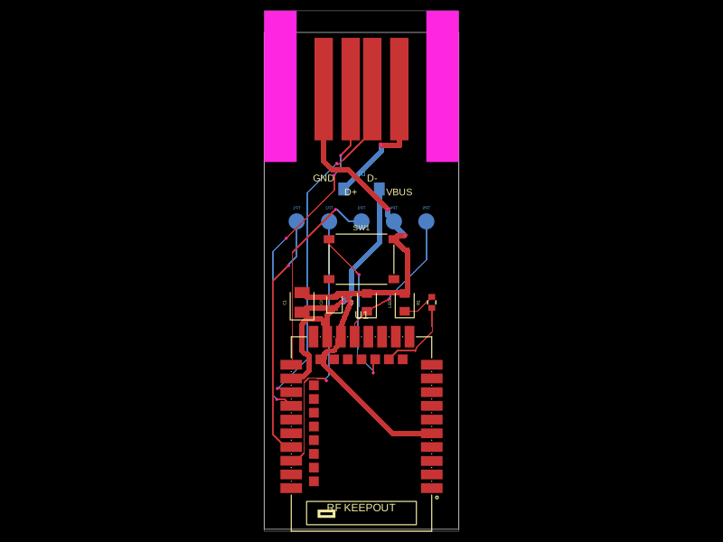 More from this authorpixalynx/keyboardThis code defines the physical layout and key components of a USB-C dongle featuring an nRF52840 microcontroller with antenna, USB-A connector, status LED, pair button, firmware debug test points, and associated passive components and interface connectors.
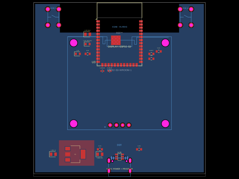 Similar packagegokul/board-v2This design integrates an ESP32-S3 Wi-Fi and Bluetooth module, a USB-C port with power and data circuitry, a USB ESD protection chip, a 3.3V voltage regulator, and an OLED display module on a PCB with associated routing and thermal copper pour layers.
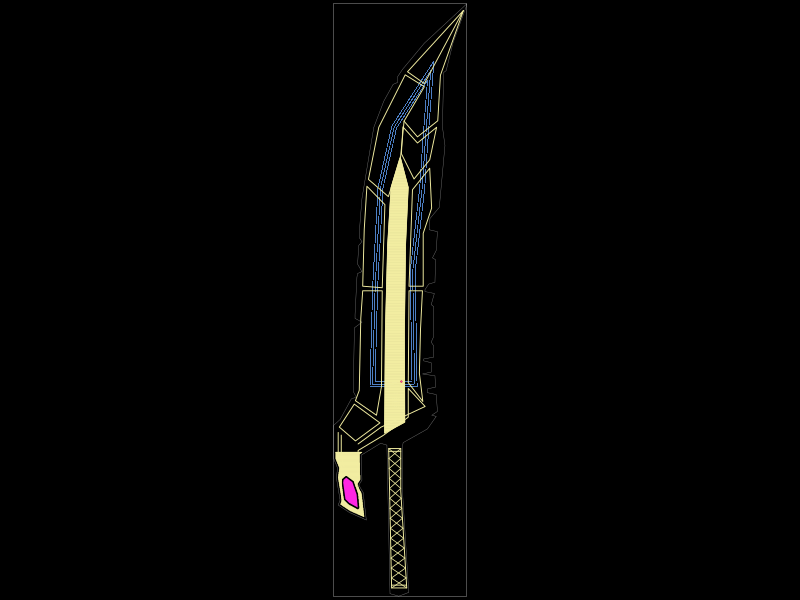 Discover something newkrishnax12/tensa-zangetsu-keychain-nfcThis code defines a PCB footprint and 3D model for an NFC-enabled electronic component featuring an NXP NT2H1311F0DTLH chip, a PCB copper coil antenna, and a custom-shaped, silkscreen-illustrated metal blade housing.