pixalynx/cm5-minimal-carrier
A 4-layer Raspberry Pi CM5 carrier board routes USB‑C 5V power through an RT9742 load switch with TVS protection and capacitive filtering, while providing ESD-protected HDMI output, CM5 connectors, test points, and ground/power planes.
- Version
- 0.1.1
- License
- unset
- Stars
- 0
scripts/export-kicad.py
"""Export the EMITTED tscircuit copper to KiCad for independent DRC and fabrication review.
No routing is added here. Physical vias are ordinary through-vias, never blind vias.
"""
import pcbnew as k,json,pathlib,math
R=pathlib.Path(__file__).resolve().parents[1];out=R/'output';j=json.loads((R/'dist/index/circuit.json').read_text());D=json.loads((R/'lib/design.json').read_text())
M=json.loads((R/'lib/manufacturing.json').read_text());testpoints={p['ref']:p for p in M['testPoints']}
b=k.BOARD();b.SetCopperLayerCount(4);b.GetDesignSettings().SetBoardThickness(k.FromMM(1.6))
L={'top':k.F_Cu,'inner1':k.In1_Cu,'inner2':k.In2_Cu,'bottom':k.B_Cu}
def xy(x,y):return k.VECTOR2I(k.FromMM(x+100),k.FromMM(100-y))
def pt(p):return xy(p['x'],p['y'])
def vec(w,h):return k.VECTOR2I(k.FromMM(w),k.FromMM(h))
# The same bottom-left origin is used by Gerber, drill, IPC netlist and CPL.
b.GetDesignSettings().SetAuxOrigin(xy(M['origin']['boardX'],M['origin']['boardY']))
b.GetDesignSettings().m_TentViasFront=M['tentViasTop'];b.GetDesignSettings().m_TentViasBack=M['tentViasBottom']
b.GetDesignSettings().m_SolderMaskMinWidth=k.FromMM(M['minimumMaskWebMm'])
def layers(ids):
 s=k.LSET()
 for layer in ids:s.AddLayer(layer)
 return s
N={};key={}
for n in [e for e in j if e['type']=='source_net']:
 net=k.NETINFO_ITEM(b,n['name']);b.Add(net);N[n['name']]=net;key[n['subcircuit_connectivity_map_key']]=n['name']
sc={e['source_component_id']:e for e in j if e['type']=='source_component'};sp={e['source_port_id']:e for e in j if e['type']=='source_port'};pp={e['pcb_port_id']:e for e in j if e['type']=='pcb_port'};st={e['source_trace_id']:e for e in j if e['type']=='source_trace'}
def pn(e):
 p=pp.get(e.get('pcb_port_id'));s=sp.get(p['source_port_id']) if p else None;return key.get(s.get('subcircuit_connectivity_map_key')) if s else None
fps={}
cad_models=json.loads((R/'lib/cad-models.json').read_text())
for c in [e for e in j if e['type']=='pcb_component']:
 f=k.FOOTPRINT(b);ref=sc[c['source_component_id']]['name'];f.SetReference(ref);f.SetValue(testpoints[ref]['label'] if ref in testpoints else next(p['value'] for p in D['parts'] if p['ref']==ref));f.SetPosition(pt(c['center']));f.SetLayer(L[c['layer']]);f.SetAttributes(k.FP_SMD);f.Reference().SetVisible(False);f.Value().SetVisible(False);b.Add(f);fps[c['pcb_component_id']]=f
 if ref in testpoints:
  f.SetAttributes(k.FP_EXCLUDE_FROM_BOM | k.FP_EXCLUDE_FROM_POS_FILES);continue
 part=next(p for p in D['parts'] if p['ref']==ref);model=cad_models[part['footprint']];angle=math.radians(part['rotation']);ox,oy,oz=model['offset'];rx,ry,rz=model['rotation']
 body=k.FP_3DMODEL();body.m_Filename='${KIPRJMOD}/../models/'+model['file'];body.m_Scale=k.VECTOR3D(1,1,1)
 body.m_Rotation=k.VECTOR3D(-rx,-ry,-rz-part['rotation'])
 body.m_Offset=k.VECTOR3D(part['x']-c['center']['x']+ox*math.cos(angle)-oy*math.sin(angle),part['y']-c['center']['y']+ox*math.sin(angle)+oy*math.cos(angle),oz)
 f.Models().push_back(body)
for e in [e for e in j if e['type'] in ['pcb_smtpad','pcb_plated_hole']]:
 f=fps[e['pcb_component_id']];p=k.PAD(f);p.SetNumber(next((n[3:] for n in e.get('port_hints',[]) if n.startswith('pin')),'0'));p.SetPosition(pt(e))
 if e['type']=='pcb_smtpad':
  p.SetAttribute(k.PAD_ATTRIB_SMD);circle=e['shape']=='circle';p.SetShape(k.PAD_SHAPE_CIRCLE if circle else k.PAD_SHAPE_RECT);p.SetSize(vec(e['radius']*2,e['radius']*2) if circle else vec(e['width'],e['height']));layer=L[e['layer']]
  pad_layers=[layer,k.F_Mask if layer==k.F_Cu else k.B_Mask]
  if f.GetReference() not in testpoints:pad_layers.append(k.F_Paste if layer==k.F_Cu else k.B_Paste)
  p.SetLayerSet(layers(pad_layers));p.SetOrientationDegrees(e.get('ccw_rotation',0))
 else:
  p.SetAttribute(k.PAD_ATTRIB_PTH);p.SetShape(k.PAD_SHAPE_OVAL);p.SetSize(vec(e['outer_width'],e['outer_height']));p.SetDrillShape(k.PAD_DRILL_SHAPE_OBLONG);p.SetDrillSize(vec(e['hole_width'],e['hole_height']));p.SetOrientationDegrees(e.get('ccw_rotation',0));p.SetLayerSet(layers([k.F_Cu,k.In1_Cu,k.In2_Cu,k.B_Cu,k.F_Mask,k.B_Mask]));f.SetAttributes(k.FP_THROUGH_HOLE)
 if pn(e):p.SetNet(N[pn(e)])
 p.SetLocalSolderMaskMargin(k.FromMM(.05 if f.GetReference() in testpoints else M['padMaskExpansionMm']));f.Add(p)
for i,e in enumerate(e for e in j if e['type']=='pcb_hole'):
 if e.get('pcb_component_id') in fps:f=fps[e['pcb_component_id']]
 else:
  f=k.FOOTPRINT(b);f.SetReference('H'+str(i+1));f.SetPosition(pt(e));f.Reference().SetVisible(False);f.Value().SetVisible(False);b.Add(f)
  shape=k.PCB_SHAPE(f);shape.SetShape(k.SHAPE_T_CIRCLE);shape.SetCenter(pt(e));shape.SetEnd(xy(e['x']+1.7,e['y']));shape.SetLayer(k.F_CrtYd);shape.SetWidth(k.FromMM(.05));f.Add(shape)
 p=k.PAD(f);p.SetAttribute(k.PAD_ATTRIB_NPTH);p.SetShape(k.PAD_SHAPE_CIRCLE);d=e.get('hole_diameter') or e.get('hole_width');p.SetSize(vec(d,d));p.SetDrillSize(vec(d,d));p.SetPosition(pt(e));p.SetLayerSet(layers([k.F_Cu,k.In1_Cu,k.In2_Cu,k.B_Cu,k.F_Mask,k.B_Mask]));f.Add(p)
for e in [e for e in j if e['type']=='pcb_trace']:
 name=key[st[e['source_trace_id']]['subcircuit_connectivity_map_key']];prev=None
 for p in e['route']:
  if p['route_type']=='wire':
   if prev and prev['layer']==p['layer'] and math.hypot(prev['x']-p['x'],prev['y']-p['y'])>1e-6:
    t=k.PCB_TRACK(b);t.SetStart(pt(prev));t.SetEnd(pt(p));t.SetWidth(k.FromMM(p['width']));t.SetLayer(L[p['layer']]);t.SetNet(N[name]);b.Add(t)
   prev=p
  else:
   if prev and math.hypot(prev['x']-p['x'],prev['y']-p['y'])>1e-6:
    t=k.PCB_TRACK(b);t.SetStart(pt(prev));t.SetEnd(pt(p));t.SetWidth(k.FromMM(prev['width']));t.SetLayer(L[p['from_layer']]);t.SetNet(N[name]);b.Add(t)
   prev=dict(p,layer=p['to_layer'],width=prev['width'] if prev else .15)

seen=set()
for e in [e for e in j if e['type']=='pcb_via']:
 name=key[e['subcircuit_connectivity_map_key']];sig=(round(e['x'],6),round(e['y'],6),name)
 if sig in seen:continue
 seen.add(sig);v=k.PCB_VIA(b);v.SetPosition(pt(e));v.SetWidth(k.FromMM(e['outer_diameter']));v.SetDrill(k.FromMM(e['hole_diameter']));v.SetViaType(k.VIATYPE_THROUGH);v.SetLayerPair(k.F_Cu,k.B_Cu);v.SetNet(N[name]);v.SetFrontTentingMode(k.TENTING_MODE_TENTED);v.SetBackTentingMode(k.TENTING_MODE_TENTED);b.Add(v)
# Exact tscircuit pour outlines; KiCad independently calculates clearances and fills.
for e in [e for e in j if e['type']=='pcb_copper_pour']:
 n=next(n for n in j if n['type']=='source_net' and n['source_net_id']==e['source_net_id'])['name'];z=k.ZONE(b);z.SetLayer(L[e['layer']]);z.SetNet(N[n]);z.SetLocalClearance(k.FromMM(.2));z.SetPadConnection(k.ZONE_CONNECTION_FULL);z.SetMinThickness(k.FromMM(.1));poly=z.Outline();poly.NewOutline()
 for p in e['brep_shape']['outer_ring']['vertices']:
  q=pt(p);poly.Append(q.x,q.y)
 b.Add(z)
# Outline, physical module outline and requested labels. Copper remains unchanged.
def line(a,c,layer,w=.12,owner=None):
 s=k.PCB_SHAPE(owner or b);s.SetShape(k.SHAPE_T_SEGMENT);s.SetStart(xy(*a));s.SetEnd(xy(*c));s.SetLayer(layer);s.SetWidth(k.FromMM(w));(owner or b).Add(s)
box=[(-32,-30),(32,-30),(32,30),(-32,30),(-32,-30)]
for a,c in zip(box,box[1:]):line(a,c,k.Edge_Cuts,.05)
for e in [e for e in j if e['type']=='pcb_courtyard_outline']:
 f=fps[e['pcb_component_id']]
 for a,c in zip(e['outline'],e['outline'][1:]):line((a['x'],a['y']),(c['x'],c['y']),k.F_CrtYd if e['layer']=='top' else k.B_CrtYd,.05,f)
for e in [e for e in j if e['type']=='pcb_silkscreen_path']:
 if e.get('route'):
  for a,c in zip(e['route'],e['route'][1:]):line((a['x'],a['y']),(c['x'],c['y']),k.F_SilkS if e.get('layer','top')=='top' else k.B_SilkS,e.get('stroke_width',.12))
for e in [e for e in j if e['type']=='pcb_silkscreen_text']:
 layer=k.B_SilkS if e['layer']=='bottom' else k.F_SilkS
 t=k.PCB_TEXT(b);t.SetText(e['text']);t.SetPosition(pt(e['anchor_position']));t.SetTextSize(vec(e['font_size'],e['font_size']));t.SetTextThickness(k.FromMM(.15));t.SetLayer(layer);t.SetMirrored(layer==k.B_SilkS);b.Add(t)
b.BuildConnectivity();k.ZONE_FILLER(b).Fill(b.Zones());k.SaveBoard(str(out/'cm5-minimal.kicad_pcb'),b)
# Verify the filled reference plane at the trace centre and both copper edges.
gnd=next(z for z in b.Zones() if z.GetNetname()=='GND').GetFilledPolysList(k.In1_Cu)
miss=[];samples=0
for t in b.GetTracks():
 if isinstance(t,k.PCB_VIA) or t.GetLayer()!=k.F_Cu or not (t.GetNetname().startswith('HDMI_TX') or t.GetNetname().startswith('HDMI_CLK')):continue
 a=t.GetStart();c=t.GetEnd();dx=c.x-a.x;dy=c.y-a.y;distance=math.hypot(dx,dy)
 for i in range(max(2,math.ceil(k.ToMM(distance)/.05))+1):
  steps=max(2,math.ceil(k.ToMM(distance)/.05));fraction=i/steps
  for off in [-t.GetWidth()/2,0,t.GetWidth()/2]:
   q=k.VECTOR2I(round(a.x+dx*fraction-dy/distance*off),round(a.y+dy*fraction+dx/distance*off));samples+=1
   if not gnd.Contains(q):miss.append([t.GetNetname(),list(k.ToMM(q))])
plane_report={'groundPlaneIslands':gnd.OutlineCount(),'samples':samples,'stepMm':.05,'sampleMethod':'trace centre and both edges projected onto filled L2 GND','uncoveredSamples':miss,'powerPlaneIslands':next(z for z in b.Zones() if z.GetNetname()=='CM5_5V').GetFilledPolysList(k.In2_Cu).OutlineCount()}
(out/'plane-audit.json').write_text(json.dumps(plane_report,indent=2)+'\n')
assert not miss, 'HDMI trace copper has a void in its ground reference'
assert gnd.OutlineCount()==1,'Ground plane is disconnected'
# Embed the proposed manufacturer's stack-up; this remains an explicit release gate.
stack=json.loads((R/'lib/stackup.json').read_text())
block='\t\t(stackup\n'
for row in stack['layers']:
 block+='\t\t\t(layer "'+row['name']+'" (type "'+row['type']+'") (thickness '+str(row['thickness'])+')'
 if 'material' in row:block+=' (material "'+row['material']+'") (epsilon_r '+str(row['epsilon_r'])+') (loss_tangent 0.02)'
 block+=')\n'
block+='\t\t\t(copper_finish "ENIG")\n\t\t\t(dielectric_constraints yes)\n\t\t)\n'
file=out/'cm5-minimal.kicad_pcb';file.write_text(file.read_text().replace('\t(setup\n','\t(setup\n'+block,1))
pro={'meta':{'filename':'cm5-minimal.kicad_pro','version':1},'board':{'design_settings':{'drc_exclusions':[],'rules':{'min_clearance':.1,'min_track_width':.12,'min_via_diameter':.4,'min_through_hole_diameter':.2,'min_via_annular_width':.1,'min_hole_to_hole':.25,'min_copper_edge_clearance':.2,'min_hole_clearance':.1,'min_silk_clearance':.15,'min_text_height':1,'min_text_thickness':.15,'allow_blind_buried_vias':False,'allow_microvias':False},'rule_severities':{'clearance':'error','shorting_items':'error','unconnected_items':'error','tracks_crossing':'error','missing_courtyard':'warning'}}},'net_settings':{'classes':[{'name':'Default','clearance':.1,'track_width':.15,'via_diameter':.4,'via_drill':.2,'diff_pair_width':stack['traceWidthMm'],'diff_pair_gap':stack['traceGapMm'],'diff_pair_via_gap':.25}]}}
(out/'cm5-minimal.kicad_pro').write_text(json.dumps(pro,indent=2)+'\n')
print('Exported emitted copper:',len(fps),'components,',len(seen),'through vias; filled 2 inner planes')
Related Packages
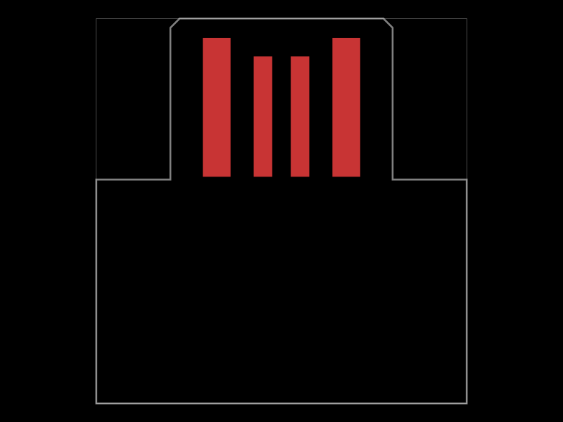 More from this authorpixalynx/edge-connectorConfigures USB-A, Micro-USB, and USB-C PCB-edge connectors with exposed copper contacts and automatically shaped, positioned board tongues.
 Similar packagegokul/usb-hub-boardA 4-layer 100×66 mm USB 2.0 hub board with a USB‑C upstream port, four protected downstream USB‑C/USB‑A ports, an integrated SD card reader, USB hub controllers, 3.3 V regulation, ESD protection, current-limited power switches, crystal oscillators, and filtering/passive components.
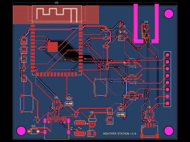 Discover something newolivergrabinski/weather-stationA compact ESP32-S3 Wi‑Fi/Bluetooth module is powered by an AP2112K 3.3 V regulator, with a JST SH connector and blue status LED.