pixalynx/cm5-minimal-carrier
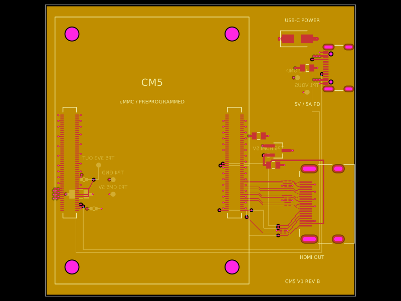
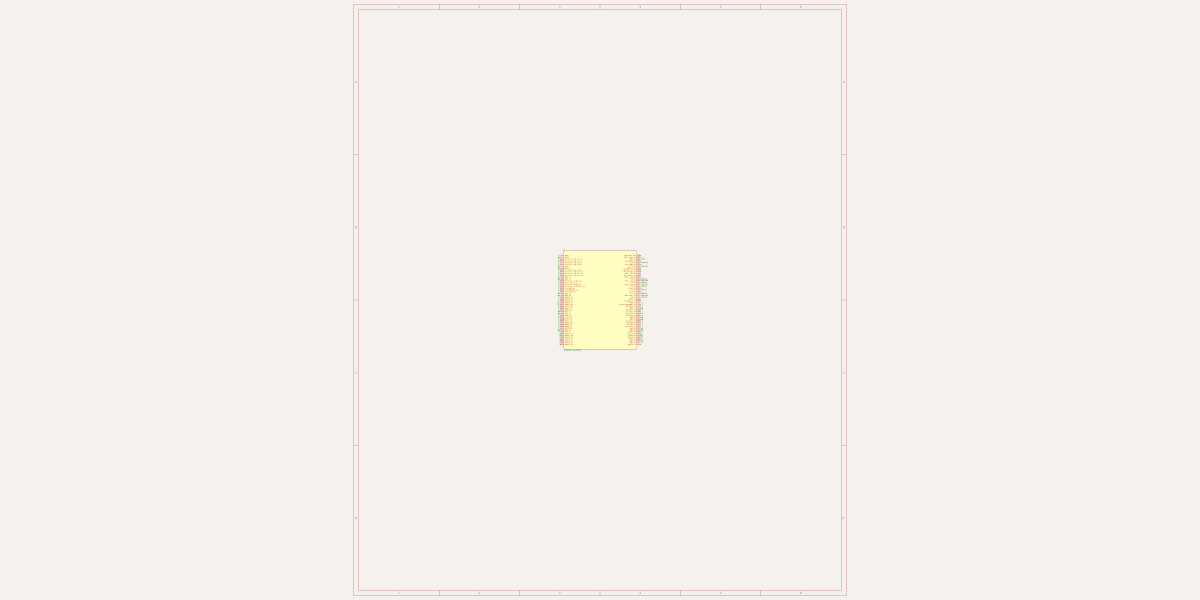
A 4-layer Raspberry Pi CM5 carrier board routes USB‑C 5V power through an RT9742 load switch with TVS protection and capacitive filtering, while providing ESD-protected HDMI output, CM5 connectors, test points, and ground/power planes.
- Version
- 0.1.1
- License
- unset
- Stars
- 0
index.circuit.tsx
PCB
Schematic
import design from './lib/design.json'
import routes from './lib/routes.json'
import { Footprint } from './lib/footprints'
import { Children } from 'react'
import cadModels from './lib/cad-models.json'
import geometry from './lib/footprints.json'
import cm5ModuleUrl from './models/cm5-module.glb'
import manufacturing from './lib/manufacturing.json'
import { RT9742SNGV, RT9742SNGVCadModel } from './imports/RT9742SNGV/RT9742SNGV'
import { SMAJ5_0A_13_F, SMAJ5_0A_13_FCadModel } from './imports/SMAJ5_0A_13_F/SMAJ5_0A_13_F'

const sections = [...new Set(design.parts.map(p => p.section))]
type PartData = typeof design.parts[number]

function Part({part:p}: {part:PartData}) {
  const index = design.parts.filter(a => a.section === p.section).indexOf(p)
  const model = cadModels[p.footprint as keyof typeof cadModels]
  const g = geometry[p.footprint as keyof typeof geometry]
  const centre = {
    x:(Math.min(...g.pads.map(a=>a.x-a.w/2))+Math.max(...g.pads.map(a=>a.x+a.w/2)))/2,
    y:(Math.min(...g.pads.map(a=>a.y-a.h/2))+Math.max(...g.pads.map(a=>a.y+a.h/2)))/2,
  }
  const rad=p.rotation*Math.PI/180
  const dx=model.cadOffset[0]-centre.x,dy=model.cadOffset[1]-centre.y
  const cadModel={objUrl:model.objUrl,mtlUrl:model.mtlUrl,modelUnitToMmScale:1,
    modelOriginPosition:{x:0,y:0,z:0},
    rotationOffset:{x:model.cadRotation[0],y:model.cadRotation[1],z:model.cadRotation[2]},
    positionOffset:{x:dx*Math.cos(rad)-dy*Math.sin(rad),y:dx*Math.sin(rad)+dy*Math.cos(rad),z:model.cadOffset[2]}}
  const nets: Record<string,string|undefined> = p.nets
  const attributes = Object.fromEntries(Object.keys(p.labels).map(n => {
    if (!(n in nets)) return [`pin${n}`, {doNotConnect:true}]
    const power = p.ref === 'U1' && n === '1'
    return [`pin${n}`, {mustBeConnected:true,
      ...(nets[n] === 'GND' ? {requiresGround:true} : {}),
      ...(power ? {requiresPower:true, requiresVoltage:5} : {})}]
  }))
  const common = {
    name:p.ref, pcbX:p.x, pcbY:p.y, pcbRotation:p.rotation,
    layer:p.layer as 'top'|'bottom', footprint:<Footprint id={p.footprint}/>,
    // Preserve reviewed copper. The imported U1 footprint has the opposite
    // orientation, so rotate its body an additional 180 degrees to match.
    cadModel: p.ref === 'U1' ? {...RT9742SNGVCadModel, pcbRotationOffset:270}
      : p.ref === 'D1' ? SMAJ5_0A_13_FCadModel : cadModel,
    schSheetName:p.section, schSectionName:p.section,
    schX:p.section === 'HDMI_ESD' || p.section.startsWith('CM5') || p.section==='USB_C_Power' || p.section==='HDMI_Output' ? 0 : (index % 3) * 7 - 7,
    schY:p.section === 'HDMI_ESD' ? -index*4 : -Math.floor(index / 3)*4,
    pinAttributes:attributes,
    manufacturerPartNumber:p.mpn, supplierPartNumbers:{lcsc:[p.lcsc],jlcpcb:[p.lcsc]},
  }
  if (p.ref.startsWith('C')) return <capacitor {...common} capacitance={p.value}/>
  // D_SMA land 1 is cathode. Use an explicit symbol: the library avalanche
  // symbol's numbered ports do not match this package's polarity.
  if (p.ref === 'D1') return <SMAJ5_0A_13_F {...common} variant="avalanche"
    pinLabels={{pin1:['cathode'],pin2:['anode']}}
    symbol={<symbol width={1.5} height={1.2}>
      <port name="cathode" pinNumber={1} schX={-.75} schY={0} direction="left"/>
      <port name="anode" pinNumber={2} schX={.75} schY={0} direction="right"/>
      <schematicpath points={[{x:-.75,y:0},{x:-.2,y:0}]} strokeWidth={.02}/>
      <schematicpath points={[{x:.2,y:0},{x:.75,y:0}]} strokeWidth={.02}/>
      <schematicpath points={[{x:-.2,y:0},{x:.2,y:.22},{x:.2,y:-.22},{x:-.2,y:0}]} strokeWidth={.02}/>
      <schematicpath points={[{x:-.32,y:-.27},{x:-.2,y:-.22},{x:-.2,y:.22},{x:-.08,y:.27}]} strokeWidth={.02}/>
      <schematictext text={p.ref} schY={.48} fontSize={.18}/>
      <schematictext text="SMAJ5.0A" schY={-.48} fontSize={.18}/>
    </symbol>}/>
  const Component = p.ref === 'U1' ? RT9742SNGV : p.ref.startsWith('J') ? 'connector' : 'chip'
  const labels = Object.fromEntries(Object.entries(p.labels).map(([n,s]) => [
    `pin${n}`, [`${s.replace(/[^A-Za-z0-9_]/g,'_')}_${p.ref === 'J2' ? 'CM5_'+(100+Number(n)) : n}`]
  ]))
  return <Component {...common} pinLabels={labels}
    schWidth={p.ref === 'J1' || p.ref === 'J2' ? 8 : p.ref==='U1'?2:6}
    schHeight={p.ref === 'J1' || p.ref === 'J2' ? 10.8 : undefined}>
    {/* Mechanical CM5 body shares J1's CAD anchor, without adding carrier pads or BOM rows. */}
    {p.ref === 'J1' && <cadmodel modelUrl={cm5ModuleUrl}
      modelUnitToMmScale={1} modelBoardNormalDirection="z+"
      modelOriginPosition={{x:0,y:0,z:0}}
      positionOffset={{x:design.moduleCenter[0]-p.x,y:design.moduleCenter[1]-p.y,z:1.5}}/>}
  </Component>
}

export default function Board() {
  return <board width={design.width} height={design.height} layers={4} thickness={1.6}
    title="CM5 MINIMAL / V1 REV B" routingDisabled schTraceAutoLabelEnabled
    pcbStyle={{viaHoleDiameter:.2,viaPadDiameter:.4}}>
    {Children.toArray(sections.map((s,i) => <schematicsheet name={s}
      displayName={`${i+1}. ${s.replaceAll('_',' ')}`}
      sheetWidth={s.startsWith('CM5') ? 500 : 600}
      sheetHeight={s.startsWith('CM5') ? 600 : 400}/>))}
    {Children.toArray(sections.map(s => <schematicsection name={s} displayName={s.replaceAll('_',' ')}/>))}
    {Children.toArray(design.nets.map(n => <net name={n} isGroundNet={n === 'GND'} isPowerNet={/5V|3V3/.test(n)}/>))}
    {design.parts.map(p => <Part key={p.ref} part={p}/>)}
    <schematicsheet name="Test_Points" displayName="8. Test points" sheetWidth={600} sheetHeight={400}/>
    <schematicsection name="Test_Points" displayName="Bare copper probe pads"/>
    {manufacturing.testPoints.map((p,i)=><testpoint key={p.ref} name={p.ref}
      pcbX={p.x} pcbY={p.y} layer="bottom" footprintVariant="pad" padShape="circle"
      padDiameter={p.diameter} cadModel={null} schSheetName="Test_Points" schSectionName="Test_Points"
      schX={(i%3)*5-5} schY={-Math.floor(i/3)*3}
      footprint={<footprint><smtpad portHints={['pin1']} shape="circle" radius={p.diameter/2}
        solderMaskMargin={.05} solderPasteMargin={-p.diameter/2}/>
        <courtyardoutline outline={[{x:-.75,y:-.75},{x:.75,y:-.75},{x:.75,y:.75},{x:-.75,y:.75},{x:-.75,y:-.75}]}/>
      </footprint>}/>)}
    {Children.toArray(manufacturing.testPoints.map(p=><netlabel connectsTo={`${p.ref}.pin1`} net={p.net} inline/>))}
    {Children.toArray(manufacturing.testPoints.map(p=><silkscreentext text={`${p.ref} ${p.label}`}
      pcbX={p.x} pcbY={p.y+1.4} layer="bottom" fontSize={1} anchorAlignment="center"/>))}
    {Children.toArray(design.parts.flatMap(p => Object.entries(p.nets).map(([n,net]) =>
      <netlabel connectsTo={`${p.ref}.pin${n}`} net={net} inline/>)))}
    {Children.toArray(routes.map((r,i) => {
      const p = [...design.parts,...manufacturing.testPoints].find(p => r.from.startsWith(p.ref+'.'))!
      const a = -('rotation' in p ? p.rotation : 0) * Math.PI/180
      return <trace name={`route_${i}`} from={r.from} to={r.to} thickness={r.width}
        pcbPath={r.path.map(q => {
          const dx=q.x-p.x, dy=q.y-p.y
          return {x:dx*Math.cos(a)-dy*Math.sin(a), y:dx*Math.sin(a)+dy*Math.cos(a),
            ...('via' in q ? {via:q.via as boolean, fromLayer:q.fromLayer as 'top', toLayer:q.toLayer as 'bottom'} : {})}
        })}/>
    }))}
    <copperpour name="L2_GND" layer="inner1" connectsTo="net.GND" unbroken clearance={.2} boardEdgeMargin={.3} useThermalReliefs={false}/>
    <copperpour name="L3_5V" layer="inner2" connectsTo="net.CM5_5V" unbroken clearance={.2} boardEdgeMargin={.3} useThermalReliefs={false}/>
    {Children.toArray(design.holes.map(([x,y]) => <hole pcbX={x} pcbY={y} diameter={2.7}/>))}
    <silkscreenpath route={[{x:-30,y:-27.5},{x:10,y:-27.5},{x:10,y:27.5},{x:-30,y:27.5},{x:-30,y:-27.5}]} strokeWidth={.15}/>
    <silkscreentext text="CM5" pcbX={-10} pcbY={14} fontSize={2} anchorAlignment="center"/>
    <silkscreentext text="eMMC / PREPROGRAMMED" pcbX={-10} pcbY={10} fontSize={1} anchorAlignment="center"/>
    <silkscreentext text="USB-C POWER" pcbX={21} pcbY={26.8} fontSize={1} anchorAlignment="center"/>
    <silkscreentext text="5V / 5A PD" pcbX={22} pcbY={9.5} fontSize={1} anchorAlignment="center"/>
    <silkscreentext text="HDMI OUT" pcbX={23} pcbY={-22} fontSize={1} anchorAlignment="center"/>
    <silkscreentext text="CM5 V1 REV B" pcbX={21} pcbY={-27} fontSize={1} anchorAlignment="center"/>
  </board>
}
Related Packages
 More from this authorpixalynx/edge-connectorConfigures USB-A, Micro-USB, and USB-C PCB-edge connectors with exposed copper contacts and automatically shaped, positioned board tongues.
 Similar packagegokul/usb-hub-boardA 4-layer 100×66 mm USB 2.0 hub board with a USB‑C upstream port, four protected downstream USB‑C/USB‑A ports, an integrated SD card reader, USB hub controllers, 3.3 V regulation, ESD protection, current-limited power switches, crystal oscillators, and filtering/passive components.
 Discover something newolivergrabinski/weather-stationA compact ESP32-S3 Wi‑Fi/Bluetooth module is powered by an AP2112K 3.3 V regulator, with a JST SH connector and blue status LED.