nater_tot/generic-motion-ctrl-v1
A 70×55 mm RP2040 motion-control board with USB‑C/3.3 V regulation, QSPI flash, dual TMC2209 stepper drivers for 12–24 V motors, encoder/limit-switch I/O, and protected power/ground hardware.
- Version
- 1.0.1
- License
- unset
- Stars
- 0
index.circuit.tsx
PCB
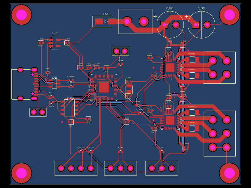
Schematic

import React from "react"
// Custom footprint for M3 Plated Through-Hole (PTH) mounting pad
// 3.2 mm hole diameter, 6.0 mm annular copper pad, tied to GND
const M3MountingPadFootprint = () => (
<footprint>
<platedhole
portHints={["pin1"]}
pcbX="0mm"
pcbY="0mm"
shape="circle"
holeDiameter="3.2mm"
outerDiameter="6.0mm"
/>
<courtyardcircle radius="3.2mm" />
</footprint>
)
// Vertical Through-Hole 5.08mm 2-Pin Screw Terminal Footprint (C407085)
const ScrewTerminal2P508Footprint = () => (
<footprint insertionDirection="from_above">
<platedhole
portHints={["pin1"]}
pcbX="-2.54mm"
pcbY="0mm"
shape="circle"
holeDiameter="1.5mm"
outerDiameter="2.8mm"
/>
<platedhole
portHints={["pin2"]}
pcbX="2.54mm"
pcbY="0mm"
shape="circle"
holeDiameter="1.5mm"
outerDiameter="2.8mm"
/>
<silkscreenrect pcbX="0mm" pcbY="0mm" width="10.16mm" height="7.5mm" />
<courtyardrect pcbX="0mm" pcbY="0mm" width="10.66mm" height="8.0mm" />
</footprint>
)
// Vertical Through-Hole Molex Mini-Fit Jr. 4.2mm 2x2 Dual-Row 4-Pin Header Footprint (Motor 1 Poka-Yoke)
const MiniFitJr2x2Footprint = () => (
<footprint insertionDirection="from_above">
<platedhole
portHints={["pin1"]}
pcbX="-2.1mm"
pcbY="2.1mm"
shape="circle"
holeDiameter="1.4mm"
outerDiameter="2.4mm"
/>
<platedhole
portHints={["pin2"]}
pcbX="2.1mm"
pcbY="2.1mm"
shape="circle"
holeDiameter="1.4mm"
outerDiameter="2.4mm"
/>
<platedhole
portHints={["pin3"]}
pcbX="-2.1mm"
pcbY="-2.1mm"
shape="circle"
holeDiameter="1.4mm"
outerDiameter="2.4mm"
/>
<platedhole
portHints={["pin4"]}
pcbX="2.1mm"
pcbY="-2.1mm"
shape="circle"
holeDiameter="1.4mm"
outerDiameter="2.4mm"
/>
<silkscreenrect pcbX="0mm" pcbY="0mm" width="9.6mm" height="9.6mm" />
<courtyardrect pcbX="0mm" pcbY="0mm" width="10.2mm" height="10.2mm" />
</footprint>
)
// Vertical Through-Hole Molex Mini-Fit Jr. 4.2mm 3x2 Dual-Row 6-Pin Header Footprint (Motor 2 Poka-Yoke)
const MiniFitJr3x2Footprint = () => (
<footprint insertionDirection="from_above">
<platedhole
portHints={["pin1"]}
pcbX="-2.1mm"
pcbY="4.2mm"
shape="circle"
holeDiameter="1.4mm"
outerDiameter="2.4mm"
/>
<platedhole
portHints={["pin2"]}
pcbX="2.1mm"
pcbY="4.2mm"
shape="circle"
holeDiameter="1.4mm"
outerDiameter="2.4mm"
/>
<platedhole
portHints={["pin3"]}
pcbX="-2.1mm"
pcbY="0mm"
shape="circle"
holeDiameter="1.4mm"
outerDiameter="2.4mm"
/>
<platedhole
portHints={["pin4"]}
pcbX="2.1mm"
pcbY="0mm"
shape="circle"
holeDiameter="1.4mm"
outerDiameter="2.4mm"
/>
<platedhole
portHints={["pin5"]}
pcbX="-2.1mm"
pcbY="-4.2mm"
shape="circle"
holeDiameter="1.4mm"
outerDiameter="2.4mm"
/>
<platedhole
portHints={["pin6"]}
pcbX="2.1mm"
pcbY="-4.2mm"
shape="circle"
holeDiameter="1.4mm"
outerDiameter="2.4mm"
/>
<silkscreenrect pcbX="0mm" pcbY="0mm" width="9.6mm" height="13.8mm" />
<courtyardrect pcbX="0mm" pcbY="0mm" width="10.2mm" height="14.4mm" />
</footprint>
)
// Vertical Through-Hole Micro-Fit 3.0 1x4 Single-Row Header Footprint (C2941545)
const MicroFit1x4Footprint = () => (
<footprint insertionDirection="from_above">
<platedhole
portHints={["pin1"]}
pcbX="-4.5mm"
pcbY="0mm"
shape="circle"
holeDiameter="1.02mm"
outerDiameter="1.8mm"
/>
<platedhole
portHints={["pin2"]}
pcbX="-1.5mm"
pcbY="0mm"
shape="circle"
holeDiameter="1.02mm"
outerDiameter="1.8mm"
/>
<platedhole
portHints={["pin3"]}
pcbX="1.5mm"
pcbY="0mm"
shape="circle"
holeDiameter="1.02mm"
outerDiameter="1.8mm"
/>
<platedhole
portHints={["pin4"]}
pcbX="4.5mm"
pcbY="0mm"
shape="circle"
holeDiameter="1.02mm"
outerDiameter="1.8mm"
/>
<silkscreenrect pcbX="0mm" pcbY="0mm" width="12.85mm" height="4.37mm" />
<courtyardrect pcbX="0mm" pcbY="0mm" width="13.35mm" height="4.87mm" />
</footprint>
)
// Vertical Through-Hole Micro-Fit 3.0 1x3 Single-Row Header Footprint (C2941546)
const MicroFit1x3Footprint = () => (
<footprint insertionDirection="from_above">
<platedhole
portHints={["pin1"]}
pcbX="-3.0mm"
pcbY="0mm"
shape="circle"
holeDiameter="1.02mm"
outerDiameter="1.8mm"
/>
<platedhole
portHints={["pin2"]}
pcbX="0mm"
pcbY="0mm"
shape="circle"
holeDiameter="1.02mm"
outerDiameter="1.8mm"
/>
<platedhole
portHints={["pin3"]}
pcbX="3.0mm"
pcbY="0mm"
shape="circle"
holeDiameter="1.02mm"
outerDiameter="1.8mm"
/>
<silkscreenrect pcbX="0mm" pcbY="0mm" width="9.85mm" height="4.37mm" />
<courtyardrect pcbX="0mm" pcbY="0mm" width="10.35mm" height="4.87mm" />
</footprint>
)
// Vertical 2-Pin 2.54mm Header Footprint for BOOTSEL / RESET (C318884)
const Header2PinFootprint = () => (
<footprint insertionDirection="from_above">
<platedhole
portHints={["pin1"]}
pcbX="-1.27mm"
pcbY="0mm"
shape="circle"
holeDiameter="1.0mm"
outerDiameter="1.7mm"
/>
<platedhole
portHints={["pin2"]}
pcbX="1.27mm"
pcbY="0mm"
shape="circle"
holeDiameter="1.0mm"
outerDiameter="1.7mm"
/>
<silkscreenrect pcbX="0mm" pcbY="0mm" width="5.08mm" height="2.54mm" />
<courtyardrect pcbX="0mm" pcbY="0mm" width="5.58mm" height="3.04mm" />
</footprint>
)
const tmc2209PinLabels = {
pin1: "OB2",
pin2: "ENN",
pin3: "GND1",
pin4: "CPO",
pin5: "CPI",
pin6: "VCP",
pin7: "SPREAD",
pin8: "V5OUT",
pin9: "MS1",
pin10: "MS2",
pin11: "DIAG",
pin12: "INDEX",
pin13: "CLK",
pin14: "PDN_UART",
pin15: "VCC_IO",
pin16: "STEP",
pin17: "VREF",
pin18: "GND2",
pin19: "DIR",
pin20: "STDBY",
pin21: "OA2",
pin22: "VS1",
pin23: "BRA",
pin24: "OA1",
pin25: "NC",
pin26: "OB1",
pin27: "BRB",
pin28: "VS2",
pin29: "EPAD",
} as const
// Precomputed Tier-2 High-Current Motor Phase (1.2mm, min 0.5mm at pad) & Sense (0.8mm) Trace Paths
// Smoothly tapers from 0.5mm at the QFN-28 pads to 1.2mm immediately upon pad exit
const motorPhasePcbTracePaths = [
{
connection: ".U_DRV1 > port.OB2",
route: [
{ route_type: "wire" as const, x: 15.0, y: 10.35, width: 0.5, start_width: 0.5, end_width: 0.5, width_interpolation_mode: "linear" as const, layer: "top" as const },
{ route_type: "wire" as const, x: 15.0, y: 10.8, width: 0.5, start_width: 0.5, end_width: 0.52, width_interpolation_mode: "linear" as const, layer: "top" as const },
{ route_type: "wire" as const, x: 15.25, y: 11.05, width: 0.52, start_width: 0.52, end_width: 0.72, width_interpolation_mode: "linear" as const, layer: "top" as const },
{ route_type: "wire" as const, x: 15.55, y: 11.35, width: 0.72, start_width: 0.72, end_width: 0.96, width_interpolation_mode: "linear" as const, layer: "top" as const },
{ route_type: "wire" as const, x: 15.9, y: 11.7, width: 0.96, start_width: 0.96, end_width: 1.2, width_interpolation_mode: "linear" as const, layer: "top" as const },
{ route_type: "wire" as const, x: 16.3, y: 12.1, width: 1.2, layer: "top" as const },
{ route_type: "wire" as const, x: 16.5, y: 12.3, width: 1.2, layer: "top" as const },
{ route_type: "wire" as const, x: 28.4, y: 12.3, width: 1.2, layer: "top" as const },
{ route_type: "wire" as const, x: 30.6, y: 10.1, width: 1.2, layer: "top" as const },
],
},
{
connection: ".U_DRV1 > port.BRB",
route: [
{ route_type: "wire" as const, x: 15.85, y: 9.0, width: 0.28, start_width: 0.28, end_width: 0.3, width_interpolation_mode: "linear" as const, layer: "top" as const },
{ route_type: "wire" as const, x: 16.2, y: 9.0, width: 0.3, start_width: 0.3, end_width: 0.3, width_interpolation_mode: "linear" as const, layer: "top" as const },
{ route_type: "wire" as const, x: 16.45, y: 9.25, width: 0.3, start_width: 0.3, end_width: 0.46, width_interpolation_mode: "linear" as const, layer: "top" as const },
{ route_type: "wire" as const, x: 16.8, y: 9.6, width: 0.46, start_width: 0.46, end_width: 0.64, width_interpolation_mode: "linear" as const, layer: "top" as const },
{ route_type: "wire" as const, x: 17.2, y: 10.0, width: 0.64, start_width: 0.64, end_width: 0.8, width_interpolation_mode: "linear" as const, layer: "top" as const },
{ route_type: "wire" as const, x: 17.6, y: 10.4, width: 0.8, layer: "top" as const },
{ route_type: "wire" as const, x: 18.7375, y: 10.4, width: 0.8, layer: "top" as const },
],
},
{
connection: ".U_DRV1 > port.OB1",
route: [
{ route_type: "wire" as const, x: 15.85, y: 8.5, width: 0.5, start_width: 0.5, end_width: 0.5, width_interpolation_mode: "linear" as const, layer: "top" as const },
{ route_type: "wire" as const, x: 16.3, y: 8.5, width: 0.5, start_width: 0.5, end_width: 0.5, width_interpolation_mode: "linear" as const, layer: "top" as const },
{ route_type: "wire" as const, x: 16.55, y: 8.5, width: 0.5, start_width: 0.5, end_width: 0.68, width_interpolation_mode: "linear" as const, layer: "top" as const },
{ route_type: "wire" as const, x: 16.85, y: 8.5, width: 0.68, start_width: 0.68, end_width: 0.88, width_interpolation_mode: "linear" as const, layer: "top" as const },
{ route_type: "wire" as const, x: 17.12, y: 8.5, width: 0.88, start_width: 0.88, end_width: 1.04, width_interpolation_mode: "linear" as const, layer: "top" as const },
{ route_type: "wire" as const, x: 17.32, y: 8.7, width: 1.04, start_width: 1.04, end_width: 1.2, width_interpolation_mode: "linear" as const, layer: "top" as const },
{ route_type: "wire" as const, x: 17.6, y: 8.7, width: 1.2, layer: "top" as const },
{ route_type: "wire" as const, x: 25.0, y: 8.7, width: 1.2, layer: "top" as const },
{ route_type: "wire" as const, x: 26.4, y: 10.1, width: 1.2, layer: "top" as const },
],
},
{
connection: ".U_DRV1 > port.OA1",
route: [
{ route_type: "wire" as const, x: 15.85, y: 7.5, width: 0.5, start_width: 0.5, end_width: 0.5, width_interpolation_mode: "linear" as const, layer: "top" as const },
{ route_type: "wire" as const, x: 16.3, y: 7.5, width: 0.5, start_width: 0.5, end_width: 0.5, width_interpolation_mode: "linear" as const, layer: "top" as const },
{ route_type: "wire" as const, x: 16.55, y: 7.5, width: 0.5, start_width: 0.5, end_width: 0.68, width_interpolation_mode: "linear" as const, layer: "top" as const },
{ route_type: "wire" as const, x: 16.85, y: 7.5, width: 0.68, start_width: 0.68, end_width: 0.88, width_interpolation_mode: "linear" as const, layer: "top" as const },
{ route_type: "wire" as const, x: 17.12, y: 7.5, width: 0.88, start_width: 0.88, end_width: 1.04, width_interpolation_mode: "linear" as const, layer: "top" as const },
{ route_type: "wire" as const, x: 17.32, y: 7.3, width: 1.04, start_width: 1.04, end_width: 1.2, width_interpolation_mode: "linear" as const, layer: "top" as const },
{ route_type: "wire" as const, x: 17.6, y: 7.3, width: 1.2, layer: "top" as const },
{ route_type: "wire" as const, x: 25.0, y: 7.3, width: 1.2, layer: "top" as const },
{ route_type: "wire" as const, x: 26.4, y: 5.9, width: 1.2, layer: "top" as const },
],
},
{
connection: ".U_DRV1 > port.BRA",
route: [
{ route_type: "wire" as const, x: 15.85, y: 7.0, width: 0.28, start_width: 0.28, end_width: 0.3, width_interpolation_mode: "linear" as const, layer: "top" as const },
{ route_type: "wire" as const, x: 16.2, y: 7.0, width: 0.3, start_width: 0.3, end_width: 0.3, width_interpolation_mode: "linear" as const, layer: "top" as const },
{ route_type: "wire" as const, x: 16.45, y: 6.75, width: 0.3, start_width: 0.3, end_width: 0.46, width_interpolation_mode: "linear" as const, layer: "top" as const },
{ route_type: "wire" as const, x: 16.8, y: 6.4, width: 0.46, start_width: 0.46, end_width: 0.64, width_interpolation_mode: "linear" as const, layer: "top" as const },
{ route_type: "wire" as const, x: 17.2, y: 6.0, width: 0.64, start_width: 0.64, end_width: 0.8, width_interpolation_mode: "linear" as const, layer: "top" as const },
{ route_type: "wire" as const, x: 17.6, y: 5.6, width: 0.8, layer: "top" as const },
{ route_type: "wire" as const, x: 18.7375, y: 5.6, width: 0.8, layer: "top" as const },
],
},
{
connection: ".U_DRV1 > port.OA2",
route: [
{ route_type: "wire" as const, x: 15.0, y: 5.65, width: 0.5, start_width: 0.5, end_width: 0.5, width_interpolation_mode: "linear" as const, layer: "top" as const },
{ route_type: "wire" as const, x: 15.0, y: 5.2, width: 0.5, start_width: 0.5, end_width: 0.52, width_interpolation_mode: "linear" as const, layer: "top" as const },
{ route_type: "wire" as const, x: 15.25, y: 4.95, width: 0.52, start_width: 0.52, end_width: 0.72, width_interpolation_mode: "linear" as const, layer: "top" as const },
{ route_type: "wire" as const, x: 15.55, y: 4.65, width: 0.72, start_width: 0.72, end_width: 0.96, width_interpolation_mode: "linear" as const, layer: "top" as const },
{ route_type: "wire" as const, x: 15.9, y: 4.3, width: 0.96, start_width: 0.96, end_width: 1.2, width_interpolation_mode: "linear" as const, layer: "top" as const },
{ route_type: "wire" as const, x: 16.3, y: 3.9, width: 1.2, layer: "top" as const },
{ route_type: "wire" as const, x: 16.5, y: 3.7, width: 1.2, layer: "top" as const },
{ route_type: "wire" as const, x: 28.4, y: 3.7, width: 1.2, layer: "top" as const },
{ route_type: "wire" as const, x: 30.6, y: 5.9, width: 1.2, layer: "top" as const },
],
},
{
connection: ".U_DRV2 > port.OB2",
route: [
{ route_type: "wire" as const, x: 15.0, y: -5.65, width: 0.5, start_width: 0.5, end_width: 0.5, width_interpolation_mode: "linear" as const, layer: "top" as const },
{ route_type: "wire" as const, x: 15.0, y: -5.2, width: 0.5, start_width: 0.5, end_width: 0.52, width_interpolation_mode: "linear" as const, layer: "top" as const },
{ route_type: "wire" as const, x: 15.25, y: -4.95, width: 0.52, start_width: 0.52, end_width: 0.72, width_interpolation_mode: "linear" as const, layer: "top" as const },
{ route_type: "wire" as const, x: 15.55, y: -4.65, width: 0.72, start_width: 0.72, end_width: 0.96, width_interpolation_mode: "linear" as const, layer: "top" as const },
{ route_type: "wire" as const, x: 15.9, y: -4.3, width: 0.96, start_width: 0.96, end_width: 1.2, width_interpolation_mode: "linear" as const, layer: "top" as const },
{ route_type: "wire" as const, x: 16.3, y: -3.9, width: 1.2, layer: "top" as const },
{ route_type: "wire" as const, x: 16.5, y: -3.7, width: 1.2, layer: "top" as const },
{ route_type: "wire" as const, x: 26.5, y: -3.7, width: 1.2, layer: "top" as const },
{ route_type: "wire" as const, x: 30.6, y: -7.8, width: 1.2, layer: "top" as const },
],
},
{
connection: ".U_DRV2 > port.BRB",
route: [
{ route_type: "wire" as const, x: 15.85, y: -7.0, width: 0.28, start_width: 0.28, end_width: 0.3, width_interpolation_mode: "linear" as const, layer: "top" as const },
{ route_type: "wire" as const, x: 16.2, y: -7.0, width: 0.3, start_width: 0.3, end_width: 0.3, width_interpolation_mode: "linear" as const, layer: "top" as const },
{ route_type: "wire" as const, x: 16.45, y: -6.75, width: 0.3, start_width: 0.3, end_width: 0.46, width_interpolation_mode: "linear" as const, layer: "top" as const },
{ route_type: "wire" as const, x: 16.8, y: -6.4, width: 0.46, start_width: 0.46, end_width: 0.64, width_interpolation_mode: "linear" as const, layer: "top" as const },
{ route_type: "wire" as const, x: 17.2, y: -6.0, width: 0.64, start_width: 0.64, end_width: 0.8, width_interpolation_mode: "linear" as const, layer: "top" as const },
{ route_type: "wire" as const, x: 17.6, y: -5.6, width: 0.8, layer: "top" as const },
{ route_type: "wire" as const, x: 18.7375, y: -5.6, width: 0.8, layer: "top" as const },
],
},
{
connection: ".U_DRV2 > port.OB1",
route: [
{ route_type: "wire" as const, x: 15.85, y: -7.5, width: 0.5, start_width: 0.5, end_width: 0.5, width_interpolation_mode: "linear" as const, layer: "top" as const },
{ route_type: "wire" as const, x: 16.3, y: -7.5, width: 0.5, start_width: 0.5, end_width: 0.5, width_interpolation_mode: "linear" as const, layer: "top" as const },
{ route_type: "wire" as const, x: 16.55, y: -7.5, width: 0.5, start_width: 0.5, end_width: 0.68, width_interpolation_mode: "linear" as const, layer: "top" as const },
{ route_type: "wire" as const, x: 16.85, y: -7.5, width: 0.68, start_width: 0.68, end_width: 0.88, width_interpolation_mode: "linear" as const, layer: "top" as const },
{ route_type: "wire" as const, x: 17.12, y: -7.5, width: 0.88, start_width: 0.88, end_width: 1.04, width_interpolation_mode: "linear" as const, layer: "top" as const },
{ route_type: "wire" as const, x: 17.32, y: -7.3, width: 1.04, start_width: 1.04, end_width: 1.2, width_interpolation_mode: "linear" as const, layer: "top" as const },
{ route_type: "wire" as const, x: 17.6, y: -7.3, width: 1.2, layer: "top" as const },
{ route_type: "wire" as const, x: 25.9, y: -7.3, width: 1.2, layer: "top" as const },
{ route_type: "wire" as const, x: 26.4, y: -7.8, width: 1.2, layer: "top" as const },
],
},
{
connection: ".U_DRV2 > port.OA1",
route: [
{ route_type: "wire" as const, x: 15.85, y: -8.5, width: 0.5, start_width: 0.5, end_width: 0.5, width_interpolation_mode: "linear" as const, layer: "top" as const },
{ route_type: "wire" as const, x: 16.3, y: -8.5, width: 0.5, start_width: 0.5, end_width: 0.5, width_interpolation_mode: "linear" as const, layer: "top" as const },
{ route_type: "wire" as const, x: 16.55, y: -8.5, width: 0.5, start_width: 0.5, end_width: 0.68, width_interpolation_mode: "linear" as const, layer: "top" as const },
{ route_type: "wire" as const, x: 16.85, y: -8.5, width: 0.68, start_width: 0.68, end_width: 0.88, width_interpolation_mode: "linear" as const, layer: "top" as const },
{ route_type: "wire" as const, x: 17.12, y: -8.5, width: 0.88, start_width: 0.88, end_width: 1.04, width_interpolation_mode: "linear" as const, layer: "top" as const },
{ route_type: "wire" as const, x: 17.32, y: -8.7, width: 1.04, start_width: 1.04, end_width: 1.2, width_interpolation_mode: "linear" as const, layer: "top" as const },
{ route_type: "wire" as const, x: 17.6, y: -8.7, width: 1.2, layer: "top" as const },
{ route_type: "wire" as const, x: 23.1, y: -8.7, width: 1.2, layer: "top" as const },
{ route_type: "wire" as const, x: 26.4, y: -12.0, width: 1.2, layer: "top" as const },
],
},
{
connection: ".U_DRV2 > port.BRA",
route: [
{ route_type: "wire" as const, x: 15.85, y: -9.0, width: 0.28, start_width: 0.28, end_width: 0.3, width_interpolation_mode: "linear" as const, layer: "top" as const },
{ route_type: "wire" as const, x: 16.2, y: -9.0, width: 0.3, start_width: 0.3, end_width: 0.3, width_interpolation_mode: "linear" as const, layer: "top" as const },
{ route_type: "wire" as const, x: 16.45, y: -9.25, width: 0.3, start_width: 0.3, end_width: 0.46, width_interpolation_mode: "linear" as const, layer: "top" as const },
{ route_type: "wire" as const, x: 16.8, y: -9.6, width: 0.46, start_width: 0.46, end_width: 0.64, width_interpolation_mode: "linear" as const, layer: "top" as const },
{ route_type: "wire" as const, x: 17.2, y: -10.0, width: 0.64, start_width: 0.64, end_width: 0.8, width_interpolation_mode: "linear" as const, layer: "top" as const },
{ route_type: "wire" as const, x: 17.6, y: -10.4, width: 0.8, layer: "top" as const },
{ route_type: "wire" as const, x: 18.7375, y: -10.4, width: 0.8, layer: "top" as const },
],
},
{
connection: ".U_DRV2 > port.OA2",
route: [
{ route_type: "wire" as const, x: 15.0, y: -10.35, width: 0.5, start_width: 0.5, end_width: 0.5, width_interpolation_mode: "linear" as const, layer: "top" as const },
{ route_type: "wire" as const, x: 15.0, y: -10.8, width: 0.5, start_width: 0.5, end_width: 0.52, width_interpolation_mode: "linear" as const, layer: "top" as const },
{ route_type: "wire" as const, x: 15.25, y: -11.05, width: 0.52, start_width: 0.52, end_width: 0.72, width_interpolation_mode: "linear" as const, layer: "top" as const },
{ route_type: "wire" as const, x: 15.55, y: -11.35, width: 0.72, start_width: 0.72, end_width: 0.96, width_interpolation_mode: "linear" as const, layer: "top" as const },
{ route_type: "wire" as const, x: 15.9, y: -11.7, width: 0.96, start_width: 0.96, end_width: 1.2, width_interpolation_mode: "linear" as const, layer: "top" as const },
{ route_type: "wire" as const, x: 16.3, y: -12.1, width: 1.2, layer: "top" as const },
{ route_type: "wire" as const, x: 16.5, y: -12.3, width: 1.2, layer: "top" as const },
{ route_type: "wire" as const, x: 21.5, y: -12.3, width: 1.2, layer: "top" as const },
{ route_type: "wire" as const, x: 23.3, y: -14.1, width: 1.2, layer: "top" as const },
{ route_type: "wire" as const, x: 28.5, y: -14.1, width: 1.2, layer: "top" as const },
{ route_type: "wire" as const, x: 30.6, y: -12.0, width: 1.2, layer: "top" as const },
],
},
{
connection: ".U_DRV1 > port.CPI",
route: [
{ route_type: "wire" as const, x: 13.0, y: 10.35, width: 0.24, layer: "top" as const },
{ route_type: "wire" as const, x: 13.0, y: 12.04, width: 0.24, layer: "top" as const },
{ route_type: "wire" as const, x: 12.74, y: 12.3, width: 0.24, layer: "top" as const },
],
},
{
connection: ".U_DRV1 > port.CPO",
route: [
{ route_type: "wire" as const, x: 13.5, y: 10.35, width: 0.24, layer: "top" as const },
{ route_type: "wire" as const, x: 13.5, y: 12.04, width: 0.24, layer: "top" as const },
{ route_type: "wire" as const, x: 13.76, y: 12.3, width: 0.24, layer: "top" as const },
],
},
{
connection: ".U_DRV1 > port.VCP",
route: [
{ route_type: "wire" as const, x: 12.5, y: 10.35, width: 0.24, layer: "top" as const },
{ route_type: "wire" as const, x: 12.5, y: 11.2, width: 0.24, layer: "top" as const },
{ route_type: "wire" as const, x: 12.0, y: 11.7, width: 0.24, layer: "top" as const },
{ route_type: "wire" as const, x: 12.0, y: 14.06, width: 0.24, layer: "top" as const },
{ route_type: "wire" as const, x: 12.74, y: 14.8, width: 0.24, layer: "top" as const },
],
},
{
connection: ".U_DRV1 > port.V5OUT",
route: [
{ route_type: "wire" as const, x: 11.15, y: 9.5, width: 0.24, layer: "top" as const },
{ route_type: "wire" as const, x: 8.49, y: 9.5, width: 0.24, layer: "top" as const },
{ route_type: "wire" as const, x: 6.99, y: 11.0, width: 0.24, layer: "top" as const },
],
},
{
connection: ".U_DRV2 > port.CPI",
route: [
{ route_type: "wire" as const, x: 13.0, y: -5.65, width: 0.24, layer: "top" as const },
{ route_type: "wire" as const, x: 13.0, y: -3.96, width: 0.24, layer: "top" as const },
{ route_type: "wire" as const, x: 12.74, y: -3.7, width: 0.24, layer: "top" as const },
],
},
{
connection: ".U_DRV2 > port.CPO",
route: [
{ route_type: "wire" as const, x: 13.5, y: -5.65, width: 0.24, layer: "top" as const },
{ route_type: "wire" as const, x: 13.5, y: -3.96, width: 0.24, layer: "top" as const },
{ route_type: "wire" as const, x: 13.76, y: -3.7, width: 0.24, layer: "top" as const },
],
},
{
connection: ".U_DRV2 > port.VCP",
route: [
{ route_type: "wire" as const, x: 12.5, y: -5.65, width: 0.24, layer: "top" as const },
{ route_type: "wire" as const, x: 12.5, y: -4.8, width: 0.24, layer: "top" as const },
{ route_type: "wire" as const, x: 12.0, y: -4.3, width: 0.24, layer: "top" as const },
{ route_type: "wire" as const, x: 12.0, y: -1.94, width: 0.24, layer: "top" as const },
{ route_type: "wire" as const, x: 12.74, y: -1.2, width: 0.24, layer: "top" as const },
],
},
{
connection: ".U_DRV2 > port.V5OUT",
route: [
{ route_type: "wire" as const, x: 11.15, y: -6.5, width: 0.24, layer: "top" as const },
{ route_type: "wire" as const, x: 8.49, y: -6.5, width: 0.24, layer: "top" as const },
{ route_type: "wire" as const, x: 6.99, y: -5.0, width: 0.24, layer: "top" as const },
],
},
]
// Precomputed Tier-3 High-Voltage & High-Current VMOT Motor Power Paths (1.5mm trunk, >= 0.5mm everywhere)
// All 14 VMOT ports belong to a single merged SimpleRouteConnection; 13 leaf-peeling paths connect all 14 endpoints.
const vmotPowerPcbTracePaths = [
{
connection: ".D_TVS > port.cathode",
route: [
{ route_type: "wire" as const, x: -4.0, y: 22.0, width: 1.5, layer: "top" as const },
{ route_type: "wire" as const, x: 0.46, y: 22.0, width: 1.5, layer: "top" as const },
],
},
{
connection: ".J_VMOT > port.VMOT",
route: [
{ route_type: "wire" as const, x: 0.46, y: 22.0, width: 1.5, layer: "top" as const },
{ route_type: "wire" as const, x: 3.06, y: 19.4, width: 1.5, layer: "top" as const },
{ route_type: "wire" as const, x: 10.15, y: 19.4, width: 1.5, layer: "top" as const },
{ route_type: "wire" as const, x: 11.75, y: 21.0, width: 1.5, layer: "top" as const },
],
},
{
connection: ".C_BK2 > port.pos",
route: [
{ route_type: "wire" as const, x: 21.25, y: 21.0, width: 1.5, layer: "top" as const },
{ route_type: "wire" as const, x: 19.05, y: 23.2, width: 1.5, layer: "top" as const },
{ route_type: "wire" as const, x: 13.95, y: 23.2, width: 1.5, layer: "top" as const },
{ route_type: "wire" as const, x: 11.75, y: 21.0, width: 1.5, layer: "top" as const },
],
},
{
connection: ".C_BK1 > port.pos",
route: [
{ route_type: "wire" as const, x: 11.75, y: 21.0, width: 0.54, layer: "top" as const },
{ route_type: "wire" as const, x: 11.75, y: 17.61, width: 0.54, layer: "top" as const },
{ route_type: "wire" as const, x: 13.76, y: 15.6, width: 0.54, layer: "top" as const },
{ route_type: "wire" as const, x: 13.76, y: 14.8, width: 0.54, layer: "top" as const },
],
},
{
connection: ".C_VCP1 > port.pin2",
route: [
{ route_type: "wire" as const, x: 13.76, y: 14.8, width: 0.54, layer: "top" as const },
{ route_type: "wire" as const, x: 16.99, y: 14.8, width: 0.54, layer: "top" as const },
],
},
{
connection: ".U_DRV1 > port.VS2",
route: [
{ route_type: "wire" as const, x: 15.85, y: 9.5, width: 0.5, layer: "top" as const },
{ route_type: "via" as const, x: 15.85, y: 10.1, from_layer: "top" as const, to_layer: "bottom" as const, via_diameter: 0.6, via_hole_diameter: 0.3 },
{ route_type: "wire" as const, x: 16.4, y: 10.65, width: 0.54, layer: "bottom" as const },
{ route_type: "via" as const, x: 16.4, y: 13.4, from_layer: "bottom" as const, to_layer: "top" as const, via_diameter: 0.6, via_hole_diameter: 0.3 },
{ route_type: "wire" as const, x: 16.99, y: 13.99, width: 0.54, layer: "top" as const },
{ route_type: "wire" as const, x: 16.99, y: 14.8, width: 0.54, layer: "top" as const },
],
},
{
connection: ".C_VS1B > port.pin1",
route: [
{ route_type: "wire" as const, x: 16.99, y: 14.8, width: 0.54, layer: "top" as const },
{ route_type: "wire" as const, x: 16.99, y: 15.6, width: 0.54, layer: "top" as const },
{ route_type: "via" as const, x: 17.5, y: 15.6, from_layer: "top" as const, to_layer: "bottom" as const, via_diameter: 0.6, via_hole_diameter: 0.3 },
{ route_type: "via" as const, x: 17.5, y: 2.3, from_layer: "bottom" as const, to_layer: "top" as const, via_diameter: 0.6, via_hole_diameter: 0.3 },
{ route_type: "wire" as const, x: 16.99, y: 2.3, width: 0.54, layer: "top" as const },
{ route_type: "wire" as const, x: 16.99, y: 1.5, width: 0.54, layer: "top" as const },
],
},
{
connection: ".U_DRV1 > port.VS1",
route: [
{ route_type: "wire" as const, x: 15.85, y: 6.5, width: 0.5, layer: "top" as const },
{ route_type: "via" as const, x: 15.85, y: 5.9, from_layer: "top" as const, to_layer: "bottom" as const, via_diameter: 0.6, via_hole_diameter: 0.3 },
{ route_type: "wire" as const, x: 16.4, y: 5.35, width: 0.54, layer: "bottom" as const },
{ route_type: "via" as const, x: 16.4, y: 2.6, from_layer: "bottom" as const, to_layer: "top" as const, via_diameter: 0.6, via_hole_diameter: 0.3 },
{ route_type: "wire" as const, x: 16.99, y: 2.01, width: 0.54, layer: "top" as const },
{ route_type: "wire" as const, x: 16.99, y: 1.5, width: 0.54, layer: "top" as const },
],
},
{
connection: ".C_VS1A > port.pin1",
route: [
{ route_type: "wire" as const, x: 16.99, y: 1.5, width: 0.54, layer: "top" as const },
{ route_type: "wire" as const, x: 16.99, y: -1.5, width: 0.54, layer: "top" as const },
],
},
{
connection: ".C_VCP2 > port.pin2",
route: [
{ route_type: "wire" as const, x: 13.76, y: -1.2, width: 0.54, layer: "top" as const },
{ route_type: "wire" as const, x: 13.76, y: -0.4, width: 0.54, layer: "top" as const },
{ route_type: "via" as const, x: 14.0, y: -0.16, from_layer: "top" as const, to_layer: "bottom" as const, via_diameter: 0.6, via_hole_diameter: 0.3 },
{ route_type: "via" as const, x: 15.65, y: -0.16, from_layer: "bottom" as const, to_layer: "top" as const, via_diameter: 0.6, via_hole_diameter: 0.3 },
{ route_type: "wire" as const, x: 16.99, y: -1.5, width: 0.54, layer: "top" as const },
],
},
{
connection: ".U_DRV2 > port.VS2",
route: [
{ route_type: "wire" as const, x: 15.85, y: -6.5, width: 0.5, layer: "top" as const },
{ route_type: "via" as const, x: 15.85, y: -5.9, from_layer: "top" as const, to_layer: "bottom" as const, via_diameter: 0.6, via_hole_diameter: 0.3 },
{ route_type: "wire" as const, x: 16.4, y: -5.35, width: 0.54, layer: "bottom" as const },
{ route_type: "via" as const, x: 16.4, y: -2.6, from_layer: "bottom" as const, to_layer: "top" as const, via_diameter: 0.6, via_hole_diameter: 0.3 },
{ route_type: "wire" as const, x: 16.99, y: -2.01, width: 0.54, layer: "top" as const },
{ route_type: "wire" as const, x: 16.99, y: -1.5, width: 0.54, layer: "top" as const },
],
},
{
connection: ".C_VS2B > port.pin1",
route: [
{ route_type: "wire" as const, x: 16.99, y: -1.5, width: 0.54, layer: "top" as const },
{ route_type: "wire" as const, x: 16.99, y: -0.7, width: 0.54, layer: "top" as const },
{ route_type: "via" as const, x: 17.5, y: -0.7, from_layer: "top" as const, to_layer: "bottom" as const, via_diameter: 0.6, via_hole_diameter: 0.3 },
{ route_type: "via" as const, x: 17.5, y: -17.34, from_layer: "bottom" as const, to_layer: "top" as const, via_diameter: 0.6, via_hole_diameter: 0.3 },
{ route_type: "wire" as const, x: 17.84, y: -17.0, width: 0.54, layer: "top" as const },
{ route_type: "wire" as const, x: 17.84, y: -16.2, width: 0.54, layer: "top" as const },
],
},
{
connection: ".U_DRV2 > port.VS1",
route: [
{ route_type: "wire" as const, x: 15.85, y: -9.5, width: 0.5, layer: "top" as const },
{ route_type: "via" as const, x: 15.85, y: -10.1, from_layer: "top" as const, to_layer: "bottom" as const, via_diameter: 0.6, via_hole_diameter: 0.3 },
{ route_type: "wire" as const, x: 16.4, y: -10.65, width: 0.54, layer: "bottom" as const },
{ route_type: "via" as const, x: 16.4, y: -14.76, from_layer: "bottom" as const, to_layer: "top" as const, via_diameter: 0.6, via_hole_diameter: 0.3 },
{ route_type: "wire" as const, x: 17.84, y: -16.2, width: 0.54, layer: "top" as const },
],
},
]
export default () => (
<board
title="generic-motion-ctrl-v1"
width="70mm"
height="55mm"
layers={2}
routeRemaining={true}
>
{/* =====================================================================
SCHEMATIC SECTIONS
===================================================================== */}
<schematicsection name="USB_Power" displayName="USB-C & 3.3V LDO Regulation" />
<schematicsection name="VMOT_Power" displayName="12V-24V Motor Power & Protection" />
<schematicsection name="MCU_Core" displayName="RP2040 MCU, QSPI Flash & Clock" />
<schematicsection name="Stepper_Driver_1" displayName="TMC2209 Axis 1 Driver (Addr 0x00)" />
<schematicsection name="Stepper_Driver_2" displayName="TMC2209 Axis 2 Driver (Addr 0x01)" />
<schematicsection name="Sensors_IO" displayName="I2C Encoder & Optical Limit Gates" />
{/* =====================================================================
MECHANICAL: 4x M3 Plated Through-Hole (PTH) Mounting Pads (Tied to GND)
3.2 mm hole, 6.0 mm annular pad, inset 3.5 mm from 70x55 mm corners
===================================================================== */}
<chip
name="MH1"
footprint={<M3MountingPadFootprint />}
doNotPlace
pcbX={-31.5}
pcbY={24.0}
schSectionName="VMOT_Power"
schX={-32}
schY={-16}
pinLabels={{ pin1: "GND" }}
pinAttributes={{ GND: { requiresGround: true } }}
/>
<chip
name="MH2"
footprint={<M3MountingPadFootprint />}
doNotPlace
pcbX={31.5}
pcbY={24.0}
schSectionName="VMOT_Power"
schX={-29}
schY={-16}
pinLabels={{ pin1: "GND" }}
pinAttributes={{ GND: { requiresGround: true } }}
/>
<chip
name="MH3"
footprint={<M3MountingPadFootprint />}
doNotPlace
pcbX={-31.5}
pcbY={-24.0}
schSectionName="VMOT_Power"
schX={-26}
schY={-16}
pinLabels={{ pin1: "GND" }}
pinAttributes={{ GND: { requiresGround: true } }}
/>
<chip
name="MH4"
footprint={<M3MountingPadFootprint />}
doNotPlace
pcbX={31.5}
pcbY={-24.0}
schSectionName="VMOT_Power"
schX={-23}
schY={-16}
pinLabels={{ pin1: "GND" }}
pinAttributes={{ GND: { requiresGround: true } }}
/>
{/* =====================================================================
SECTION 1: USB-C & 3.3V LDO REGULATION (Left Edge on PCB)
===================================================================== */}
<connector
name="J_USB"
standard="usb_c"
manufacturerPartNumber="TYPE-C-31-M-12"
supplierPartNumbers={{ jlcpcb: ["C2765186"] }}
pcbX={-29.2}
pcbY={3.0}
pcbRotation={270}
schSectionName="USB_Power"
schX={-30}
schY={8}
schWidth={1.55}
/>
{/* 2x 5.1k CC Pull-Down Resistors (C23186) - split above/below USB data lanes */}
<resistor
name="R_CC1"
resistance="5.1k"
footprint="0402"
supplierPartNumbers={{ jlcpcb: ["C23186"] }}
pcbX={-23.5}
pcbY={6.5}
pcbRotation={0}
schSectionName="USB_Power"
schX={-25}
schY={4}
schRotation={-90}
/>
<resistor
name="R_CC2"
resistance="5.1k"
footprint="0402"
supplierPartNumbers={{ jlcpcb: ["C23186"] }}
pcbX={-22.5}
pcbY={-0.8}
pcbRotation={0}
schSectionName="USB_Power"
schX={-23}
schY={4}
schRotation={-90}
/>
{/* USBLC6-2SC6 ESD Protection Array (C85364) aligned with USB D+/D- */}
<chip
name="U_ESD"
manufacturerPartNumber="USBLC6-2SC6"
supplierPartNumbers={{ jlcpcb: ["C85364", "C2827654"] }}
footprint="sot23_6"
pcbX={-21.5}
pcbY={3.2}
schSectionName="USB_Power"
schX={-20}
schY={8}
pinLabels={{
pin1: "IO1",
pin2: "GND",
pin3: "IO2",
pin4: "IO2_OUT",
pin5: "VBUS",
pin6: "IO1_OUT",
}}
pinAttributes={{
VBUS: { requiresPower: true },
GND: { requiresGround: true },
}}
schPinArrangement={{
leftSide: { pins: ["IO1", "IO2"], direction: "top-to-bottom" },
rightSide: { pins: ["IO1_OUT", "IO2_OUT"], direction: "top-to-bottom" },
topSide: { pins: ["VBUS"], direction: "left-to-right" },
bottomSide: { pins: ["GND"], direction: "left-to-right" },
}}
/>
{/* 2x 27 Ohm USB D+/D- Series Damping Resistors (C22883) */}
<resistor
name="R_USB_DM"
resistance="27"
footprint="0402"
supplierPartNumbers={{ jlcpcb: ["C22883"] }}
pcbX={-16.5}
pcbY={4.15}
schSectionName="USB_Power"
schX={-15}
schY={9}
/>
<resistor
name="R_USB_DP"
resistance="27"
footprint="0402"
supplierPartNumbers={{ jlcpcb: ["C22883"] }}
pcbX={-16.5}
pcbY={2.25}
schSectionName="USB_Power"
schX={-15}
schY={7}
/>
{/* AP2112K-3.3 SOT-23-5 3.3V LDO Regulator (C51118) */}
<chip
name="U_LDO"
manufacturerPartNumber="AP2112K-3.3TRG1"
supplierPartNumbers={{ jlcpcb: ["C51118"] }}
footprint="sot23_5"
pcbX={-21.5}
pcbY={15.5}
schSectionName="USB_Power"
schX={-20}
schY={15}
pinLabels={{
pin1: "VIN",
pin2: "GND",
pin3: "EN",
pin4: "NC",
pin5: "VOUT",
}}
pinAttributes={{
VIN: { requiresPower: true },
EN: { requiresPower: true },
VOUT: { providesPower: true },
GND: { requiresGround: true },
NC: { doNotConnect: true },
}}
schPinArrangement={{
leftSide: { pins: ["VIN", "EN"], direction: "top-to-bottom" },
rightSide: { pins: ["VOUT", "NC"], direction: "top-to-bottom" },
bottomSide: { pins: ["GND"], direction: "left-to-right" },
}}
/>
<capacitor
name="C_IN"
capacitance="1uF"
footprint="0402"
supplierPartNumbers={{ jlcpcb: ["C15849"] }}
pcbX={-25.5}
pcbY={15.5}
schSectionName="USB_Power"
schX={-24}
schY={15}
schRotation={-90}
/>
<capacitor
name="C_OUT"
capacitance="2.2uF"
footprint="0402"
supplierPartNumbers={{ jlcpcb: ["C23630"] }}
pcbX={-17.5}
pcbY={15.5}
schSectionName="USB_Power"
schX={-16.0}
schY={15}
schRotation={-90}
/>
{/* =====================================================================
SECTION 2: 12V-24V DC MOTOR POWER & PROTECTION (Top Edge on PCB)
===================================================================== */}
<connector
name="J_VMOT"
manufacturerPartNumber="WJ500V-5.08-2P"
supplierPartNumbers={{ jlcpcb: ["C407085"] }}
footprint={<ScrewTerminal2P508Footprint />}
pcbX={3.0}
pcbY={22.0}
schSectionName="VMOT_Power"
schX={-30}
schY={-8}
pinLabels={{
pin1: "VMOT",
pin2: "GND",
}}
schPinArrangement={{
topSide: { pins: ["VMOT"], direction: "left-to-right" },
bottomSide: { pins: ["GND"], direction: "left-to-right" },
}}
/>
{/* SMAJ28A Unidirectional TVS Diode across VMOT/GND (C80362) */}
<diode
name="D_TVS"
manufacturerPartNumber="SMAJ28A"
supplierPartNumbers={{ jlcpcb: ["C80362"] }}
footprint="sma"
variant="tvs"
pcbX={-6.0}
pcbY={22.0}
schSectionName="VMOT_Power"
schX={-26.5}
schY={-8}
schRotation={90}
/>
{/* 2x 220uF 35V Low-ESR Bulk Electrolytic Capacitors across VMOT/GND */}
<capacitor
name="C_BK1"
capacitance="220uF"
maxVoltageRating="35V"
polarized
footprint="electrolytic_d8mm_p3.5mm"
supplierPartNumbers={{ jlcpcb: ["C2063"] }}
pcbX={13.5}
pcbY={21.0}
schSectionName="VMOT_Power"
schX={-23.5}
schY={-8}
schRotation={-90}
/>
<capacitor
name="C_BK2"
capacitance="220uF"
maxVoltageRating="35V"
polarized
footprint="electrolytic_d8mm_p3.5mm"
supplierPartNumbers={{ jlcpcb: ["C2063"] }}
pcbX={23.0}
pcbY={21.0}
schSectionName="VMOT_Power"
schX={-21.5}
schY={-8}
schRotation={-90}
/>
{/* =====================================================================
SECTION 3: RP2040 MCU, 16Mbit QSPI NOR FLASH & 12MHz CRYSTAL
U_MCU rotated 90 deg CCW so USB/QSPI face Left, GPIO0..7 face Bottom,
and XIN/XOUT face Right into dedicated crystal island.
===================================================================== */}
<chip
name="U_MCU"
manufacturerPartNumber="RP2040"
supplierPartNumbers={{ jlcpcb: ["C2040"] }}
footprint="qfn56_thermalpad3.1mmx3.1mm_p0.4mm_h7.9mm_pw0.2mm_pl0.85mm"
pcbX={-6.5}
pcbY={2.0}
pcbRotation={90}
schSectionName="MCU_Core"
schX={0}
schY={2}
schWidth={2.11}
schHeight={3.925}
pinLabels={{
pin1: "IOVDD6",
pin2: "GPIO0",
pin3: "GPIO1",
pin4: "GPIO2",
pin5: "GPIO3",
pin6: "GPIO4",
pin7: "GPIO5",
pin8: "GPIO6",
pin9: "GPIO7",
pin10: "IOVDD5",
pin11: "GPIO8",
pin12: "GPIO9",
pin13: "GPIO10",
pin14: "GPIO11",
pin15: "GPIO12",
pin16: "GPIO13",
pin17: "GPIO14",
pin18: "GPIO15",
pin19: "TESTEN",
pin20: "XIN",
pin21: "XOUT",
pin22: "IOVDD4",
pin23: "DVDD2",
pin24: "SWCLK",
pin25: "SWD",
pin26: "RUN",
pin27: "GPIO16",
pin28: "GPIO17",
pin29: "GPIO18",
pin30: "GPIO19",
pin31: "GPIO20",
pin32: "GPIO21",
pin33: "IOVDD3",
pin34: "GPIO22",
pin35: "GPIO23",
pin36: "GPIO24",
pin37: "GPIO25",
pin38: "GPIO26_ADC0",
pin39: "GPIO27_ADC1",
pin40: "GPIO28_ADC2",
pin41: "GPIO29_ADC3",
pin42: "IOVDD2",
pin43: "ADC_AVDD",
pin44: "VREG_IN",
pin45: "VREG_VOUT",
pin46: "USB_DM",
pin47: "USB_DP",
pin48: "USB_VDD",
pin49: "IOVDD1",
pin50: "DVDD1",
pin51: "QSPI_SD3",
pin52: "QSPI_SCLK",
pin53: "QSPI_SD0",
pin54: "QSPI_SD2",
pin55: "QSPI_SD1",
pin56: "QSPI_SS",
pin57: "GND",
}}
pinAttributes={{
IOVDD1: { requiresPower: true },
IOVDD2: { requiresPower: true },
IOVDD3: { requiresPower: true },
IOVDD4: { requiresPower: true },
IOVDD5: { requiresPower: true },
IOVDD6: { requiresPower: true },
USB_VDD: { requiresPower: true },
ADC_AVDD: { requiresPower: true },
VREG_IN: { requiresPower: true },
VREG_VOUT: { providesPower: true },
DVDD1: { requiresPower: true },
DVDD2: { requiresPower: true },
GND: { requiresGround: true },
TESTEN: { requiresGround: true },
}}
schPinArrangement={{
topSide: {
pins: [
"IOVDD1",
"IOVDD2",
"IOVDD3",
"IOVDD4",
"IOVDD5",
"IOVDD6",
"USB_VDD",
"ADC_AVDD",
"VREG_IN",
],
direction: "left-to-right",
},
leftSide: {
pins: [
"USB_DP",
"USB_DM",
"QSPI_SS",
"QSPI_SCLK",
"QSPI_SD0",
"QSPI_SD1",
"QSPI_SD2",
"QSPI_SD3",
"XIN",
"XOUT",
"RUN",
],
direction: "top-to-bottom",
},
rightSide: {
pins: [
"GPIO0",
"GPIO1",
"GPIO4",
"GPIO2",
"GPIO3",
"GPIO6",
"GPIO7",
"VREG_VOUT",
"DVDD1",
"DVDD2",
],
direction: "top-to-bottom",
},
bottomSide: {
pins: ["GND", "TESTEN"],
direction: "left-to-right",
},
}}
/>
{/* 16Mbit QSPI NOR Flash W25Q16JVSSIQ (SOIC-8, C82981) aligned with QSPI pins */}
<chip
name="U_FLASH"
manufacturerPartNumber="W25Q16JVSSIQ"
supplierPartNumbers={{ jlcpcb: ["C82981", "C82317"] }}
footprint="soic8_p1.27mm"
pcbX={-17.0}
pcbY={-4.2}
pcbRotation={0}
schSectionName="MCU_Core"
schX={-8}
schY={4}
schWidth={1.38}
pinLabels={{
pin1: "CS",
pin2: "IO1",
pin3: "IO2",
pin4: "GND",
pin5: "IO0",
pin6: "CLK",
pin7: "IO3",
pin8: "VCC",
}}
pinAttributes={{
VCC: { requiresPower: true },
GND: { requiresGround: true },
}}
schPinArrangement={{
topSide: { pins: ["VCC"], direction: "left-to-right" },
rightSide: {
pins: ["CS", "CLK", "IO0", "IO1", "IO2", "IO3"],
direction: "top-to-bottom",
},
bottomSide: { pins: ["GND"], direction: "left-to-right" },
}}
/>
<via
name="VIA_FLS_GND"
fromLayer="top"
toLayer="bottom"
holeDiameter="0.3mm"
outerDiameter="0.6mm"
pcbX={-19.15}
pcbY={-8.5}
connectsTo="net.GND"
/>
<capacitor
name="C_FLS"
capacitance="100nF"
footprint="0402"
supplierPartNumbers={{ jlcpcb: ["C14663"] }}
pcbX={-16.7}
pcbY={-8.5}
pcbRotation={180}
schSectionName="USB_Power"
schX={-14.25}
schY={15}
schRotation={-90}
/>
{/* BOOTSEL Header (J_BOOT, C318884) with 1k Series Resistor (C21190) to QSPI_SS_N */}
<resistor
name="R_BOOT"
resistance="1k"
footprint="0402"
supplierPartNumbers={{ jlcpcb: ["C21190"] }}
pcbX={-22.5}
pcbY={-2.5}
pcbRotation={180}
schSectionName="MCU_Core"
schX={-7.5}
schY={9}
/>
<connector
name="J_BOOT"
manufacturerPartNumber="TS-1187A-B-A-B"
supplierPartNumbers={{ jlcpcb: ["C318884"] }}
footprint={<Header2PinFootprint />}
pcbX={-26.5}
pcbY={-5.5}
pcbRotation={180}
schSectionName="MCU_Core"
schX={-11.5}
schY={9}
pinLabels={{
pin1: "BOOT",
pin2: "GND",
}}
schPinArrangement={{
topSide: { pins: ["BOOT"], direction: "left-to-right" },
bottomSide: { pins: ["GND"], direction: "left-to-right" },
}}
/>
{/* RESET Header (J_RESET, C318884) to RUN + 10k Pull-Up */}
<resistor
name="R_RUN"
resistance="10k"
footprint="0402"
supplierPartNumbers={{ jlcpcb: ["C25804"] }}
pcbX={-1.5}
pcbY={9.0}
schSectionName="MCU_Core"
schX={-5}
schY={-5}
schRotation={-90}
/>
<connector
name="J_RESET"
manufacturerPartNumber="TS-1187A-B-A-B"
supplierPartNumbers={{ jlcpcb: ["C318884"] }}
footprint={<Header2PinFootprint />}
pcbX={-1.5}
pcbY={13.0}
schSectionName="MCU_Core"
schX={-8.5}
schY={-5}
pinLabels={{
pin1: "RUN",
pin2: "GND",
}}
schPinArrangement={{
topSide: { pins: ["RUN"], direction: "left-to-right" },
bottomSide: { pins: ["GND"], direction: "left-to-right" },
}}
/>
{/* 12.000 MHz SMD Crystal (C16212) with 2x 18pF Load Caps (C1644) right next to XIN/XOUT */}
<crystal
name="Y1"
frequency="12MHz"
loadCapacitance="18pF"
manufacturerPartNumber="X322512MSB4SI"
supplierPartNumbers={{ jlcpcb: ["C16212"] }}
footprint="0805"
pcbX={1.0}
pcbY={1.6}
pcbRotation={90}
schSectionName="MCU_Core"
schX={-5.9}
schY={-1.7}
schRotation={180}
/>
<capacitor
name="C_XT1"
capacitance="18pF"
footprint="0402"
supplierPartNumbers={{ jlcpcb: ["C1644"] }}
pcbX={1.0}
pcbY={-0.6}
pcbRotation={0}
schSectionName="MCU_Core"
schX={-8.4}
schY={-2}
schRotation={-90}
/>
<capacitor
name="C_XT2"
capacitance="18pF"
footprint="0402"
supplierPartNumbers={{ jlcpcb: ["C1644"] }}
pcbX={1.0}
pcbY={3.8}
pcbRotation={0}
schSectionName="MCU_Core"
schX={-3.4}
schY={-2}
schRotation={-90}
/>
{/* RP2040 Core Regulator & IOVDD Decoupling Capacitors placed clear of USB/QSPI corridor */}
<capacitor
name="C_VR1"
capacitance="1uF"
footprint="0402"
supplierPartNumbers={{ jlcpcb: ["C15849"] }}
pcbX={-13.5}
pcbY={8.0}
schSectionName="USB_Power"
schX={-12.5}
schY={15}
schRotation={-90}
/>
<capacitor
name="C_VR2"
capacitance="1uF"
footprint="0402"
supplierPartNumbers={{ jlcpcb: ["C15849"] }}
pcbX={-11.0}
pcbY={8.0}
schSectionName="MCU_Core"
schX={5.0}
schY={-3}
schRotation={-90}
/>
<capacitor
name="C_DVD"
capacitance="100nF"
footprint="0402"
supplierPartNumbers={{ jlcpcb: ["C14663"] }}
pcbX={-8.5}
pcbY={8.0}
schSectionName="MCU_Core"
schX={6.75}
schY={-3}
schRotation={-90}
/>
<capacitor
name="C_DC1"
capacitance="100nF"
footprint="0402"
supplierPartNumbers={{ jlcpcb: ["C14663"] }}
pcbX={-6.0}
pcbY={8.0}
pcbRotation={180}
schSectionName="USB_Power"
schX={-10.75}
schY={15}
schRotation={-90}
/>
<capacitor
name="C_DC2"
capacitance="100nF"
footprint="0402"
supplierPartNumbers={{ jlcpcb: ["C14663"] }}
pcbX={-11.5}
pcbY={-7.5}
pcbRotation={180}
schSectionName="USB_Power"
schX={-9.0}
schY={15}
schRotation={-90}
/>
<capacitor
name="C_DC3"
capacitance="100nF"
footprint="0402"
supplierPartNumbers={{ jlcpcb: ["C14663"] }}
pcbX={0.5}
pcbY={-8.5}
pcbRotation={0}
schSectionName="USB_Power"
schX={-7.25}
schY={15}
schRotation={-90}
/>
{/* =====================================================================
SECTION 4: STEPPER DRIVER 1 (TMC2209 Address 0x00, Top-Right on PCB)
Rotated 270 deg so OB2, VS2, BRB, OB1, OA1, BRA, VS1, OA2 face Right (+X)
===================================================================== */}
<chip
name="U_DRV1"
manufacturerPartNumber="TMC2209-LA"
supplierPartNumbers={{ jlcpcb: ["C517714", "C2825700"] }}
footprint="qfn28_thermalpad2.6mmx2.6mm_p0.5mm_w5.6mm_h5.6mm_pw0.24mm_pl0.7mm"
pcbX={13.5}
pcbY={8.0}
pcbRotation={270}
schSectionName="Stepper_Driver_1"
schX={20}
schY={12}
schWidth={2.045}
schHeight={3.2}
pinLabels={tmc2209PinLabels}
pinAttributes={{
VS1: { requiresPower: true },
VS2: { requiresPower: true },
VCC_IO: { requiresPower: true },
V5OUT: { providesPower: true },
GND1: { requiresGround: true },
GND2: { requiresGround: true },
EPAD: { requiresGround: true },
NC: { doNotConnect: true },
}}
schPinArrangement={{
topSide: {
pins: ["VS1", "VS2", "VCC_IO", "VCP", "V5OUT"],
direction: "left-to-right",
},
leftSide: {
pins: ["PDN_UART", "ENN", "MS1", "MS2", "STEP", "DIR", "CLK", "SPREAD"],
direction: "top-to-bottom",
},
rightSide: {
pins: ["OA1", "OA2", "OB1", "OB2", "BRA", "BRB", "CPI", "CPO"],
direction: "top-to-bottom",
},
bottomSide: {
pins: ["GND1", "GND2", "EPAD"],
direction: "left-to-right",
},
}}
/>
{/* Thermal Relief Via around U_DRV1 Ground Pad (Left side, clear of bottom/right pin rows) */}
<via
name="VIA_DRV1_1"
fromLayer="top"
toLayer="bottom"
holeDiameter="0.3mm"
outerDiameter="0.6mm"
pcbX={8.5}
pcbY={8.0}
connectsTo="net.GND"
/>
{/* Shared Single-Wire UART 1k Resistor (C21190) & Shared ENN 10k Pull-Up (C25804) */}
<resistor
name="R_UART_TX"
resistance="1k"
footprint="0402"
supplierPartNumbers={{ jlcpcb: ["C21190"] }}
pcbX={4.5}
pcbY={-6.0}
schSectionName="Stepper_Driver_1"
schX={12}
schY={14}
/>
<resistor
name="R_ENN"
resistance="10k"
footprint="0402"
supplierPartNumbers={{ jlcpcb: ["C25804"] }}
pcbX={3.8}
pcbY={-3.5}
schSectionName="Stepper_Driver_1"
schX={12}
schY={11}
schRotation={-90}
/>
{/* Driver 1 110mOhm 1206 Sense Resistors (C61706) flanking the center OB1/OA1 channel */}
<resistor
name="R_SENSE1_B"
resistance="0.11"
footprint="1206"
supplierPartNumbers={{ jlcpcb: ["C61706"] }}
pcbX={20.2}
pcbY={10.4}
schSectionName="Stepper_Driver_1"
schX={27}
schY={10}
schRotation={-90}
/>
<resistor
name="R_SENSE1_A"
resistance="0.11"
footprint="1206"
supplierPartNumbers={{ jlcpcb: ["C61706"] }}
pcbX={20.2}
pcbY={5.6}
schSectionName="Stepper_Driver_1"
schX={25}
schY={10}
schRotation={-90}
/>
{/* Driver 1 Decoupling & Charge Pump Capacitors */}
<capacitor
name="C_VS1B"
capacitance="100nF"
footprint="0402"
supplierPartNumbers={{ jlcpcb: ["C14663"] }}
pcbX={17.5}
pcbY={14.8}
schSectionName="VMOT_Power"
schX={-17.95}
schY={-8}
schRotation={-90}
/>
<capacitor
name="C_VS1A"
capacitance="100nF"
footprint="0402"
supplierPartNumbers={{ jlcpcb: ["C14663"] }}
pcbX={17.5}
pcbY={1.5}
schSectionName="VMOT_Power"
schX={-19.7}
schY={-8}
schRotation={-90}
/>
<capacitor
name="C_VIO1"
capacitance="100nF"
footprint="0402"
supplierPartNumbers={{ jlcpcb: ["C14663"] }}
pcbX={8.5}
pcbY={5.6}
pcbRotation={180}
schSectionName="USB_Power"
schX={-5.5}
schY={15}
schRotation={-90}
/>
<capacitor
name="C_CP1"
capacitance="22nF"
footprint="0402"
supplierPartNumbers={{ jlcpcb: ["C1603"] }}
pcbX={13.25}
pcbY={12.3}
schSectionName="Stepper_Driver_1"
schX={23.5}
schY={11.2}
schOrientation="vertical"
/>
<capacitor
name="C_VCP1"
capacitance="100nF"
footprint="0402"
supplierPartNumbers={{ jlcpcb: ["C14663"] }}
pcbX={13.25}
pcbY={14.8}
pcbRotation={0}
schSectionName="Stepper_Driver_1"
schX={22}
schY={18}
schRotation={-90}
/>
<capacitor
name="C_5V1"
capacitance="2.2uF"
footprint="0402"
supplierPartNumbers={{ jlcpcb: ["C23630"] }}
pcbX={7.5}
pcbY={11.0}
schSectionName="Stepper_Driver_1"
schX={24}
schY={18}
schRotation={-90}
/>
{/* Motor 1 2x2 Mini-Fit Jr. 4.2mm 4-Pin Header (Poka-Yoke Axis 1, C2941544) on Right Edge */}
<connector
name="J_MOT1"
manufacturerPartNumber="39-28-1043"
supplierPartNumbers={{ jlcpcb: ["C2941544"] }}
footprint={<MiniFitJr2x2Footprint />}
pcbX={28.5}
pcbY={8.0}
pcbRotation={180}
schSectionName="Stepper_Driver_1"
schX={31}
schY={14}
pinLabels={{
pin1: "OA2",
pin2: "OA1",
pin3: "OB2",
pin4: "OB1",
}}
/>
{/* =====================================================================
SECTION 5: STEPPER DRIVER 2 (TMC2209 Address 0x01, Bottom-Right on PCB)
Rotated 270 deg so OB2, VS2, BRB, OB1, OA1, BRA, VS1, OA2 face Right (+X)
===================================================================== */}
<chip
name="U_DRV2"
manufacturerPartNumber="TMC2209-LA"
supplierPartNumbers={{ jlcpcb: ["C517714", "C2825700"] }}
footprint="qfn28_thermalpad2.6mmx2.6mm_p0.5mm_w5.6mm_h5.6mm_pw0.24mm_pl0.7mm"
pcbX={13.5}
pcbY={-8.0}
pcbRotation={270}
schSectionName="Stepper_Driver_2"
schX={20}
schY={-6}
schWidth={2.045}
schHeight={3.2}
pinLabels={tmc2209PinLabels}
pinAttributes={{
VS1: { requiresPower: true },
VS2: { requiresPower: true },
VCC_IO: { requiresPower: true },
V5OUT: { providesPower: true },
GND1: { requiresGround: true },
GND2: { requiresGround: true },
EPAD: { requiresGround: true },
NC: { doNotConnect: true },
}}
schPinArrangement={{
topSide: {
pins: ["VS1", "VS2", "VCC_IO", "VCP", "V5OUT"],
direction: "left-to-right",
},
leftSide: {
pins: ["PDN_UART", "ENN", "MS1", "MS2", "STEP", "DIR", "CLK", "SPREAD"],
direction: "top-to-bottom",
},
rightSide: {
pins: ["OA1", "OA2", "OB1", "OB2", "BRA", "BRB", "CPI", "CPO"],
direction: "top-to-bottom",
},
bottomSide: {
pins: ["GND1", "GND2", "EPAD"],
direction: "left-to-right",
},
}}
/>
{/* Thermal Relief Via around U_DRV2 Ground Pad (Left side, clear of bottom/right pin rows) */}
<via
name="VIA_DRV2_1"
fromLayer="top"
toLayer="bottom"
holeDiameter="0.3mm"
outerDiameter="0.6mm"
pcbX={8.5}
pcbY={-8.0}
connectsTo="net.GND"
/>
{/* Driver 2 110mOhm 1206 Sense Resistors (C61706) flanking the center OB1/OA1 channel */}
<resistor
name="R_SENSE2_B"
resistance="0.11"
footprint="1206"
supplierPartNumbers={{ jlcpcb: ["C61706"] }}
pcbX={20.2}
pcbY={-5.6}
schSectionName="Stepper_Driver_2"
schX={27}
schY={-8}
schRotation={-90}
/>
<resistor
name="R_SENSE2_A"
resistance="0.11"
footprint="1206"
supplierPartNumbers={{ jlcpcb: ["C61706"] }}
pcbX={20.2}
pcbY={-10.4}
schSectionName="Stepper_Driver_2"
schX={25}
schY={-8}
schRotation={-90}
/>
{/* Driver 2 Decoupling & Charge Pump Capacitors */}
<capacitor
name="C_VS2B"
capacitance="100nF"
footprint="0402"
supplierPartNumbers={{ jlcpcb: ["C14663"] }}
pcbX={17.5}
pcbY={-1.5}
schSectionName="VMOT_Power"
schX={-14.45}
schY={-8}
schRotation={-90}
/>
<capacitor
name="C_VS2A"
capacitance="100nF"
footprint="0402"
supplierPartNumbers={{ jlcpcb: ["C14663"] }}
pcbX={18.35}
pcbY={-16.2}
pcbRotation={0}
schSectionName="VMOT_Power"
schX={-16.2}
schY={-8}
schRotation={-90}
/>
<capacitor
name="C_VIO2"
capacitance="100nF"
footprint="0402"
supplierPartNumbers={{ jlcpcb: ["C14663"] }}
pcbX={8.5}
pcbY={-10.4}
pcbRotation={180}
schSectionName="USB_Power"
schX={-3.75}
schY={15}
schRotation={-90}
/>
<capacitor
name="C_CP2"
capacitance="22nF"
footprint="0402"
supplierPartNumbers={{ jlcpcb: ["C1603"] }}
pcbX={13.25}
pcbY={-3.7}
schSectionName="Stepper_Driver_2"
schX={23.5}
schY={-6.8}
schOrientation="vertical"
/>
<capacitor
name="C_VCP2"
capacitance="100nF"
footprint="0402"
supplierPartNumbers={{ jlcpcb: ["C14663"] }}
pcbX={13.25}
pcbY={-1.2}
pcbRotation={0}
schSectionName="Stepper_Driver_2"
schX={22}
schY={0}
schRotation={-90}
/>
<capacitor
name="C_5V2"
capacitance="2.2uF"
footprint="0402"
supplierPartNumbers={{ jlcpcb: ["C23630"] }}
pcbX={7.5}
pcbY={-5.0}
schSectionName="Stepper_Driver_2"
schX={24}
schY={0}
schRotation={-90}
/>
{/* Motor 2 3x2 Mini-Fit Jr. 4.2mm 6-Pin Header (Poka-Yoke Axis 2) on Right Edge */}
<connector
name="J_MOT2"
manufacturerPartNumber="39-28-1063"
supplierPartNumbers={{ jlcpcb: ["C2941544"] }}
footprint={<MiniFitJr3x2Footprint />}
pcbX={28.5}
pcbY={-12.0}
pcbRotation={0}
schSectionName="Stepper_Driver_2"
schX={31}
schY={-4}
pinLabels={{
pin1: "OB1",
pin2: "OB2",
pin3: "OA1",
pin4: "OA2",
pin5: "GND1",
pin6: "GND2",
}}
/>
{/* =====================================================================
SECTION 6: SENSORS I/O (Bottom Edge on PCB)
- 1x4 Micro-Fit 3.0 Magnetic Rotary Encoder (C2941545) + 4.7k Pull-Ups
- 2x 1x3 Micro-Fit 3.0 Optical Limit Gates (C2941546) + 10k Pull-Ups
===================================================================== */}
<connector
name="J_ENC"
manufacturerPartNumber="43650-0415"
supplierPartNumbers={{ jlcpcb: ["C2941545"] }}
footprint={<MicroFit1x4Footprint />}
pcbX={-15.0}
pcbY={-22.5}
schSectionName="Sensors_IO"
schX={-8}
schY={-16}
pinLabels={{
pin1: "VCC_3V3",
pin2: "GND",
pin3: "I2C1_SDA",
pin4: "I2C1_SCL",
}}
/>
<resistor
name="R_I2C_SDA"
resistance="4.7k"
footprint="0402"
supplierPartNumbers={{ jlcpcb: ["C25900"] }}
pcbX={-13.5}
pcbY={-17.5}
schSectionName="Sensors_IO"
schX={-9.5}
schY={-13.5}
schRotation={-90}
/>
<resistor
name="R_I2C_SCL"
resistance="4.7k"
footprint="0402"
supplierPartNumbers={{ jlcpcb: ["C25900"] }}
pcbX={-10.5}
pcbY={-17.5}
schSectionName="Sensors_IO"
schX={-7.5}
schY={-13.5}
schRotation={-90}
/>
<connector
name="J_LIM1"
manufacturerPartNumber="43650-0315"
supplierPartNumbers={{ jlcpcb: ["C2941546"] }}
footprint={<MicroFit1x3Footprint />}
pcbX={-1.5}
pcbY={-22.5}
schSectionName="Sensors_IO"
schX={-1}
schY={-16}
pinLabels={{
pin1: "VCC_3V3",
pin2: "GND",
pin3: "SIG",
}}
/>
<resistor
name="R_LIM1"
resistance="10k"
footprint="0402"
supplierPartNumbers={{ jlcpcb: ["C25804"] }}
pcbX={-1.5}
pcbY={-17.5}
schSectionName="Sensors_IO"
schX={-1}
schY={-13.5}
schRotation={-90}
/>
<connector
name="J_LIM2"
manufacturerPartNumber="43650-0315"
supplierPartNumbers={{ jlcpcb: ["C2941546"] }}
footprint={<MicroFit1x3Footprint />}
pcbX={11.0}
pcbY={-22.5}
schSectionName="Sensors_IO"
schX={5}
schY={-16}
pinLabels={{
pin1: "VCC_3V3",
pin2: "GND",
pin3: "SIG",
}}
/>
<resistor
name="R_LIM2"
resistance="10k"
footprint="0402"
supplierPartNumbers={{ jlcpcb: ["C25804"] }}
pcbX={11.0}
pcbY={-17.5}
schSectionName="Sensors_IO"
schX={5}
schY={-13.5}
schRotation={-90}
/>
{/* =====================================================================
STAGED 7-TIER ROUTING ARCHITECTURE (<autoroutingphase /> & Constraints)
===================================================================== */}
<autoroutingphase name="TIER1_CLOCKS_USB_QSPI" phaseIndex={0} />
<autoroutingphase
name="TIER2_MOTOR_PHASES"
phaseIndex={1}
pcbTracePaths={motorPhasePcbTracePaths}
/>
<autoroutingphase
name="TIER3_VMOT_POWER"
phaseIndex={2}
pcbTracePaths={vmotPowerPcbTracePaths}
/>
<autoroutingphase name="TIER4_SENSE_AND_I2C" phaseIndex={3} />
<autoroutingphase name="TIER5_LOGIC_POWER" phaseIndex={4} />
<autoroutingphase name="TIER6_PULSED_CONTROL" phaseIndex={5} />
<autoroutingphase name="TIER7_STATIC_CONTROL_IO" phaseIndex={6} />
{/* =====================================================================
TIER 1 (Phase 0): High-Speed Clocks & Critical Differential Pairs
- Shortest direct line-of-sight paths on TOP layer
===================================================================== */}
{/* 1A. 12.000 MHz Crystal & 18pF Load Capacitors (Top Layer) */}
<trace
name="XTAL_XIN"
from="U_MCU.XIN"
to="Y1.pin1"
width="0.2mm"
routingPhaseIndex={0}
/>
<trace
name="XTAL_XOUT"
from="U_MCU.XOUT"
to="Y1.pin2"
width="0.2mm"
routingPhaseIndex={0}
/>
<trace
name="XTAL_C1"
from="Y1.pin1"
to="C_XT1.pin1"
width="0.2mm"
routingPhaseIndex={0}
/>
<trace
name="XTAL_C2"
from="Y1.pin2"
to="C_XT2.pin1"
width="0.2mm"
routingPhaseIndex={0}
/>
{/* 1B. USB 2.0 Differential Data Pair (Top Layer, Untangled Planar) */}
<trace
name="USB_DM_IN"
from="J_USB.DM2"
to="U_ESD.IO1"
width="0.15mm"
routingPhaseIndex={0}
/>
<trace
name="USB_DP_IN"
from="J_USB.DP2"
to="U_ESD.IO2"
width="0.15mm"
routingPhaseIndex={0}
/>
<trace
name="USB_DM_ESD"
from="U_ESD.IO1_OUT"
to="R_USB_DM.pin1"
width="0.2mm"
routingPhaseIndex={0}
/>
<trace
name="USB_DP_ESD"
from="U_ESD.IO2_OUT"
to="R_USB_DP.pin1"
width="0.2mm"
routingPhaseIndex={0}
/>
<trace
name="USB_DM_MCU"
from="R_USB_DM.pin2"
to="U_MCU.USB_DM"
width="0.2mm"
routingPhaseIndex={0}
/>
<trace
name="USB_DP_MCU"
from="R_USB_DP.pin2"
to="U_MCU.USB_DP"
width="0.2mm"
routingPhaseIndex={0}
/>
{/* 1C. QSPI NOR Flash High-Frequency Interface (Top Layer) */}
<trace
name="QSPI_SS"
from="U_MCU.QSPI_SS"
to="U_FLASH.CS"
width="0.15mm"
routingPhaseIndex={0}
/>
<trace
name="QSPI_SD1"
from="U_MCU.QSPI_SD1"
to="U_FLASH.IO1"
width="0.2mm"
routingPhaseIndex={0}
/>
<trace
name="QSPI_SD2"
from="U_MCU.QSPI_SD2"
to="U_FLASH.IO2"
width="0.2mm"
routingPhaseIndex={0}
/>
<trace
name="QSPI_SD0"
from="U_MCU.QSPI_SD0"
to="U_FLASH.IO0"
width="0.2mm"
routingPhaseIndex={0}
/>
<trace
name="QSPI_SCLK"
from="U_MCU.QSPI_SCLK"
to="U_FLASH.CLK"
width="0.15mm"
routingPhaseIndex={0}
/>
<trace
name="QSPI_SD3"
from="U_MCU.QSPI_SD3"
to="U_FLASH.IO3"
width="0.15mm"
routingPhaseIndex={0}
/>
{/* =====================================================================
TIER 2 (Phase 1): High-Current Inductive Motor Phase Lines
- 1.2mm channel width via motorPhasePcbTracePaths (tapers from >= 0.5mm at QFN-28 pads)
===================================================================== */}
<trace
name="MOT1_OB2"
from="U_DRV1.OB2"
to="J_MOT1.OB2"
width="0.5mm"
routingPhaseIndex={1}
/>
<trace
name="MOT1_OB1"
from="U_DRV1.OB1"
to="J_MOT1.OB1"
width="0.5mm"
routingPhaseIndex={1}
/>
<trace
name="MOT1_OA1"
from="U_DRV1.OA1"
to="J_MOT1.OA1"
width="0.5mm"
routingPhaseIndex={1}
/>
<trace
name="MOT1_OA2"
from="U_DRV1.OA2"
to="J_MOT1.OA2"
width="0.5mm"
routingPhaseIndex={1}
/>
<trace
name="MOT2_OB2"
from="U_DRV2.OB2"
to="J_MOT2.OB2"
width="0.5mm"
routingPhaseIndex={1}
/>
<trace
name="MOT2_OB1"
from="U_DRV2.OB1"
to="J_MOT2.OB1"
width="0.5mm"
routingPhaseIndex={1}
/>
<trace
name="MOT2_OA1"
from="U_DRV2.OA1"
to="J_MOT2.OA1"
width="0.5mm"
routingPhaseIndex={1}
/>
<trace
name="MOT2_OA2"
from="U_DRV2.OA2"
to="J_MOT2.OA2"
width="0.5mm"
routingPhaseIndex={1}
/>
{/* =====================================================================
TIER 3 (Phase 2): High-Voltage & High-Current Power Rails (VMOT)
- 1.5mm trunk & >= 0.5mm branches via vmotPowerPcbTracePaths
===================================================================== */}
<net name="VMOT" routingPhaseIndex={2} />
<trace from="D_TVS.cathode" to="net.VMOT" width="1.5mm" maxLength="50mm" routingPhaseIndex={2} />
<trace from="J_VMOT.VMOT" to="net.VMOT" width="1.5mm" maxLength="50mm" routingPhaseIndex={2} />
<trace from="C_BK1.pos" to="net.VMOT" width="1.5mm" maxLength="50mm" routingPhaseIndex={2} />
<trace from="C_BK2.pos" to="net.VMOT" width="1.5mm" maxLength="50mm" routingPhaseIndex={2} />
<trace from="C_VCP1.pin2" to="net.VMOT" width="0.54mm" maxLength="50mm" routingPhaseIndex={2} />
<trace from="C_VS1B.pin1" to="net.VMOT" width="0.54mm" maxLength="50mm" routingPhaseIndex={2} />
<trace from="U_DRV1.VS2" to="net.VMOT" width="0.5mm" maxLength="50mm" routingPhaseIndex={2} />
<trace from="C_VS1A.pin1" to="net.VMOT" width="0.54mm" maxLength="50mm" routingPhaseIndex={2} />
<trace from="U_DRV1.VS1" to="net.VMOT" width="0.5mm" maxLength="50mm" routingPhaseIndex={2} />
<trace from="C_VS2B.pin1" to="net.VMOT" width="0.54mm" maxLength="50mm" routingPhaseIndex={2} />
<trace from="C_VCP2.pin2" to="net.VMOT" width="0.54mm" maxLength="50mm" routingPhaseIndex={2} />
<trace from="U_DRV2.VS2" to="net.VMOT" width="0.5mm" maxLength="50mm" routingPhaseIndex={2} />
<trace from="C_VS2A.pin1" to="net.VMOT" width="0.54mm" maxLength="50mm" routingPhaseIndex={2} />
<trace from="U_DRV2.VS1" to="net.VMOT" width="0.5mm" maxLength="50mm" routingPhaseIndex={2} />
{/* Charge Pump & Internal 5V Regulator Decoupling Loops */}
<trace
name="DRV1_CPI"
from="U_DRV1.CPI"
to="C_CP1.pin1"
width="0.2mm"
routingPhaseIndex={1}
/>
<trace
name="DRV1_CPO"
from="U_DRV1.CPO"
to="C_CP1.pin2"
width="0.2mm"
routingPhaseIndex={1}
/>
<trace
name="DRV1_VCP"
from="U_DRV1.VCP"
to="C_VCP1.pin1"
width="0.2mm"
routingPhaseIndex={1}
/>
<trace
name="DRV1_V5OUT"
from="U_DRV1.V5OUT"
to="C_5V1.pin1"
width="0.2mm"
routingPhaseIndex={1}
/>
<trace
name="DRV2_CPI"
from="U_DRV2.CPI"
to="C_CP2.pin1"
width="0.2mm"
routingPhaseIndex={1}
/>
<trace
name="DRV2_CPO"
from="U_DRV2.CPO"
to="C_CP2.pin2"
width="0.2mm"
routingPhaseIndex={1}
/>
<trace
name="DRV2_VCP"
from="U_DRV2.VCP"
to="C_VCP2.pin1"
width="0.2mm"
routingPhaseIndex={1}
/>
<trace
name="DRV2_V5OUT"
from="U_DRV2.V5OUT"
to="C_5V2.pin1"
width="0.2mm"
routingPhaseIndex={1}
/>
{/* =====================================================================
TIER 4 (Phase 3): Sensitive Analog & Sensor Communication Busses
- Current sense BRA/BRB feedback lines (0.8mm channel width via motorPhasePcbTracePaths)
- I2C1 Magnetic Rotary Encoder bus (GPIO2/GPIO3) in quiet left-bottom zone
===================================================================== */}
<trace
name="DRV1_BRA"
from="U_DRV1.BRA"
to="R_SENSE1_A.pin1"
width="0.24mm"
routingPhaseIndex={1}
/>
<trace
name="DRV1_BRB"
from="U_DRV1.BRB"
to="R_SENSE1_B.pin1"
width="0.24mm"
routingPhaseIndex={1}
/>
<trace
name="DRV2_BRA"
from="U_DRV2.BRA"
to="R_SENSE2_A.pin1"
width="0.24mm"
routingPhaseIndex={1}
/>
<trace
name="DRV2_BRB"
from="U_DRV2.BRB"
to="R_SENSE2_B.pin1"
width="0.24mm"
routingPhaseIndex={1}
/>
<trace
name="I2C1_SDA_MCU"
from="U_MCU.GPIO2"
to="R_I2C_SDA.pin2"
width="0.25mm"
routingPhaseIndex={3}
/>
<trace
name="I2C1_SDA_CONN"
from="R_I2C_SDA.pin2"
to="J_ENC.I2C1_SDA"
width="0.25mm"
routingPhaseIndex={3}
/>
<trace
name="I2C1_SCL_MCU"
from="U_MCU.GPIO3"
to="R_I2C_SCL.pin2"
width="0.25mm"
routingPhaseIndex={3}
/>
<trace
name="I2C1_SCL_CONN"
from="R_I2C_SCL.pin2"
to="J_ENC.I2C1_SCL"
width="0.25mm"
routingPhaseIndex={3}
/>
{/* =====================================================================
TIER 5 (Phase 4): Low-Voltage Logic Power Rails (VBUS_5V, V1_1, VCC_3V3)
- Routed through local decoupling caps before surrounding signals
===================================================================== */}
<trace from="J_USB.VBUS1" to="net.VBUS_5V" routingPhaseIndex={4} />
<trace from="J_USB.VBUS2" to="net.VBUS_5V" routingPhaseIndex={4} />
<trace from="U_ESD.VBUS" to="net.VBUS_5V" width="0.25mm" routingPhaseIndex={4} />
<trace from="C_IN.pin1" to="net.VBUS_5V" width="0.25mm" routingPhaseIndex={4} />
<trace from="U_LDO.VIN" to="net.VBUS_5V" width="0.25mm" routingPhaseIndex={4} />
<trace from="U_LDO.EN" to="net.VBUS_5V" width="0.25mm" routingPhaseIndex={4} />
<trace
name="V1_1_VREG_OUT"
from="U_MCU.VREG_VOUT"
to="C_VR2.pin1"
width="0.15mm"
maxLength="25mm"
routingPhaseIndex={4}
/>
<trace
name="V1_1_CAPS"
from="C_VR2.pin1"
to="C_DVD.pin1"
width="0.15mm"
maxLength="25mm"
routingPhaseIndex={4}
/>
<trace
name="V1_1_DVDD1"
from="C_VR2.pin1"
to="U_MCU.DVDD1"
width="0.15mm"
maxLength="25mm"
routingPhaseIndex={4}
/>
<trace
name="V1_1_DVDD2"
from="C_DVD.pin1"
to="U_MCU.DVDD2"
width="0.15mm"
maxLength="25mm"
routingPhaseIndex={4}
/>
<trace from="U_LDO.VOUT" to="net.VCC_3V3" width="0.25mm" routingPhaseIndex={4} />
<trace from="C_OUT.pin1" to="net.VCC_3V3" width="0.25mm" routingPhaseIndex={4} />
<trace from="C_VR1.pin1" to="net.VCC_3V3" width="0.2mm" routingPhaseIndex={4} />
<trace from="C_DC1.pin1" to="net.VCC_3V3" width="0.2mm" routingPhaseIndex={4} />
<trace from="C_DC2.pin1" to="net.VCC_3V3" width="0.2mm" routingPhaseIndex={4} />
<trace from="C_DC3.pin1" to="net.VCC_3V3" width="0.2mm" routingPhaseIndex={4} />
<trace from="C_FLS.pin1" to="net.VCC_3V3" width="0.2mm" routingPhaseIndex={4} />
<trace from="C_VIO1.pin1" to="net.VCC_3V3" width="0.2mm" routingPhaseIndex={4} />
<trace from="C_VIO2.pin1" to="net.VCC_3V3" width="0.2mm" routingPhaseIndex={4} />
<trace from="U_MCU.IOVDD1" to="net.VCC_3V3" width="0.2mm" routingPhaseIndex={4} />
<trace from="U_MCU.IOVDD2" to="net.VCC_3V3" width="0.2mm" routingPhaseIndex={4} />
<trace from="U_MCU.IOVDD3" to="net.VCC_3V3" width="0.2mm" routingPhaseIndex={4} />
<trace from="U_MCU.IOVDD4" to="net.VCC_3V3" width="0.2mm" routingPhaseIndex={4} />
<trace from="U_MCU.IOVDD5" to="net.VCC_3V3" width="0.2mm" routingPhaseIndex={4} />
<trace from="U_MCU.IOVDD6" to="net.VCC_3V3" width="0.2mm" routingPhaseIndex={4} />
<trace from="U_MCU.USB_VDD" to="net.VCC_3V3" width="0.2mm" routingPhaseIndex={4} />
<trace from="U_MCU.ADC_AVDD" to="net.VCC_3V3" width="0.2mm" routingPhaseIndex={4} />
<trace from="U_MCU.VREG_IN" to="net.VCC_3V3" width="0.2mm" routingPhaseIndex={4} />
<trace from="U_FLASH.VCC" to="net.VCC_3V3" width="0.2mm" routingPhaseIndex={4} />
<trace from="U_DRV1.VCC_IO" to="net.VCC_3V3" width="0.2mm" routingPhaseIndex={4} />
<trace from="U_DRV2.VCC_IO" to="net.VCC_3V3" width="0.2mm" routingPhaseIndex={4} />
<trace from="J_ENC.VCC_3V3" to="net.VCC_3V3" width="0.25mm" routingPhaseIndex={4} />
<trace from="J_LIM1.VCC_3V3" to="net.VCC_3V3" width="0.25mm" routingPhaseIndex={4} />
<trace from="J_LIM2.VCC_3V3" to="net.VCC_3V3" width="0.25mm" routingPhaseIndex={4} />
<trace from="R_ENN.pin1" to="net.VCC_3V3" width="0.2mm" routingPhaseIndex={4} />
<trace from="U_DRV2.MS1" to="net.VCC_3V3" width="0.2mm" routingPhaseIndex={4} />
<trace from="R_RUN.pin1" to="net.VCC_3V3" width="0.2mm" routingPhaseIndex={4} />
<trace from="R_I2C_SDA.pin1" to="net.VCC_3V3" width="0.2mm" routingPhaseIndex={4} />
<trace from="R_I2C_SCL.pin1" to="net.VCC_3V3" width="0.2mm" routingPhaseIndex={4} />
<trace from="R_LIM1.pin1" to="net.VCC_3V3" width="0.2mm" routingPhaseIndex={4} />
<trace from="R_LIM2.pin1" to="net.VCC_3V3" width="0.2mm" routingPhaseIndex={4} />
{/* =====================================================================
TIER 6 (Phase 5): Fast Digital Driver Enable & Pulsed Control Lines
===================================================================== */}
<trace
name="ENN_MCU"
from="U_MCU.GPIO4"
to="R_ENN.pin2"
width="0.15mm"
routingPhaseIndex={5}
/>
<trace
name="ENN_DRV1"
from="R_ENN.pin2"
to="U_DRV1.ENN"
width="0.15mm"
routingPhaseIndex={5}
/>
<trace
name="ENN_DRV2"
from="R_ENN.pin2"
to="U_DRV2.ENN"
width="0.15mm"
routingPhaseIndex={5}
/>
{/* =====================================================================
TIER 7 (Phase 6): Static Digital Control, Configuration, and Low-Speed I/O
- Shared UART, MS1/MS2/STEP/DIR strapping, Limit Switches, BOOT/RESET, GND
===================================================================== */}
<trace
name="USB_DM_JOIN"
from="J_USB.DM1"
to="J_USB.DM2"
width="0.15mm"
routingPhaseIndex={6}
/>
<trace
name="USB_DP_JOIN"
from="J_USB.DP1"
to="J_USB.DP2"
width="0.15mm"
routingPhaseIndex={6}
/>
<trace
name="UART_TX_MCU"
from="U_MCU.GPIO0"
to="R_UART_TX.pin1"
width="0.2mm"
routingPhaseIndex={6}
/>
<trace
name="UART_RX_MCU"
from="U_MCU.GPIO1"
to="R_UART_TX.pin2"
width="0.2mm"
routingPhaseIndex={6}
/>
<trace
name="UART_DRV1"
from="R_UART_TX.pin2"
to="U_DRV1.PDN_UART"
width="0.2mm"
routingPhaseIndex={6}
/>
<trace
name="UART_DRV2"
from="R_UART_TX.pin2"
to="U_DRV2.PDN_UART"
width="0.2mm"
routingPhaseIndex={6}
/>
<trace from="U_DRV1.STEP" to="net.GND" routingPhaseIndex={6} />
<trace from="U_DRV1.DIR" to="net.GND" routingPhaseIndex={6} />
<trace from="U_DRV1.CLK" to="net.GND" routingPhaseIndex={6} />
<trace from="U_DRV1.SPREAD" to="net.GND" routingPhaseIndex={6} />
<trace from="U_DRV1.MS1" to="net.GND" routingPhaseIndex={6} />
<trace from="U_DRV1.MS2" to="net.GND" routingPhaseIndex={6} />
<trace from="U_DRV2.STEP" to="net.GND" routingPhaseIndex={6} />
<trace from="U_DRV2.DIR" to="net.GND" routingPhaseIndex={6} />
<trace from="U_DRV2.CLK" to="net.GND" routingPhaseIndex={6} />
<trace from="U_DRV2.SPREAD" to="net.GND" routingPhaseIndex={6} />
<trace from="U_DRV2.MS2" to="net.GND" routingPhaseIndex={6} />
<trace
name="BOOT_CS"
from="U_FLASH.CS"
to="R_BOOT.pin1"
routingPhaseIndex={6}
/>
<trace
name="BOOT_HDR"
from="R_BOOT.pin2"
to="J_BOOT.BOOT"
routingPhaseIndex={6}
/>
<trace
name="RUN_PULL"
from="R_RUN.pin2"
to="U_MCU.RUN"
routingPhaseIndex={6}
/>
<trace
name="RUN_HDR"
from="J_RESET.RUN"
to="U_MCU.RUN"
routingPhaseIndex={6}
/>
<trace
name="USB_CC1"
from="J_USB.CC1"
to="R_CC1.pin1"
routingPhaseIndex={6}
/>
<trace
name="USB_CC2"
from="J_USB.CC2"
to="R_CC2.pin1"
routingPhaseIndex={6}
/>
<trace
name="LIM1_SIG_MCU"
from="J_LIM1.SIG"
to="U_MCU.GPIO6"
routingPhaseIndex={6}
/>
<trace
name="LIM1_PULL"
from="R_LIM1.pin2"
to="U_MCU.GPIO6"
routingPhaseIndex={6}
/>
<trace
name="LIM2_SIG_MCU"
from="J_LIM2.SIG"
to="U_MCU.GPIO7"
routingPhaseIndex={6}
/>
<trace
name="LIM2_PULL"
from="R_LIM2.pin2"
to="U_MCU.GPIO7"
routingPhaseIndex={6}
/>
{/* Ground Returns (Tied to Continuous Bottom GND Pour & Thermal Vias) */}
<trace from="MH1.GND" to="net.GND" routingPhaseIndex={6} />
<trace from="MH2.GND" to="net.GND" routingPhaseIndex={6} />
<trace from="MH3.GND" to="net.GND" routingPhaseIndex={6} />
<trace from="MH4.GND" to="net.GND" routingPhaseIndex={6} />
<trace from="J_USB.GND1" to="net.GND" routingPhaseIndex={6} />
<trace from="J_USB.GND2" to="net.GND" routingPhaseIndex={6} />
<trace from="R_CC1.pin2" to="net.GND" routingPhaseIndex={6} />
<trace from="R_CC2.pin2" to="net.GND" routingPhaseIndex={6} />
<trace from="U_ESD.GND" to="net.GND" routingPhaseIndex={6} />
<trace from="U_LDO.GND" to="net.GND" routingPhaseIndex={6} />
<trace from="C_IN.pin2" to="net.GND" routingPhaseIndex={6} />
<trace from="C_OUT.pin2" to="net.GND" routingPhaseIndex={6} />
<trace from="J_VMOT.GND" to="net.GND" maxLength="35mm" routingPhaseIndex={6} />
<trace from="D_TVS.anode" to="net.GND" maxLength="35mm" routingPhaseIndex={6} />
<trace from="C_BK1.neg" to="net.GND" maxLength="35mm" routingPhaseIndex={6} />
<trace from="C_BK2.neg" to="net.GND" maxLength="35mm" routingPhaseIndex={6} />
<trace from="U_MCU.GND" to="net.GND" routingPhaseIndex={6} />
<trace from="U_MCU.TESTEN" to="net.GND" routingPhaseIndex={6} />
<trace from="C_VR1.pin2" to="net.GND" maxLength="25mm" routingPhaseIndex={6} />
<trace from="C_VR2.pin2" to="net.GND" maxLength="25mm" routingPhaseIndex={6} />
<trace from="C_DVD.pin2" to="net.GND" maxLength="25mm" routingPhaseIndex={6} />
<trace from="C_DC1.pin2" to="net.GND" maxLength="25mm" routingPhaseIndex={6} />
<trace from="C_DC2.pin2" to="net.GND" routingPhaseIndex={6} />
<trace from="C_DC3.pin2" to="net.GND" routingPhaseIndex={6} />
<trace from="U_FLASH.GND" to="net.GND" routingPhaseIndex={6} />
<trace from="C_FLS.pin2" to="net.GND" routingPhaseIndex={6} />
<trace from="J_BOOT.GND" to="net.GND" routingPhaseIndex={6} />
<trace from="J_RESET.GND" to="net.GND" routingPhaseIndex={6} />
<trace from="C_XT1.pin2" to="net.GND" routingPhaseIndex={6} />
<trace from="C_XT2.pin2" to="net.GND" routingPhaseIndex={6} />
<trace from="U_DRV1.GND1" to="net.GND" routingPhaseIndex={6} />
<trace from="U_DRV1.GND2" to="net.GND" routingPhaseIndex={6} />
<trace from="U_DRV1.EPAD" to="net.GND" routingPhaseIndex={6} />
<trace from="C_VS1A.pin2" to="net.GND" maxLength="35mm" routingPhaseIndex={6} />
<trace from="C_VS1B.pin2" to="net.GND" maxLength="35mm" routingPhaseIndex={6} />
<trace from="C_VIO1.pin2" to="net.GND" routingPhaseIndex={6} />
<trace from="C_5V1.pin2" to="net.GND" routingPhaseIndex={6} />
<trace from="R_SENSE1_A.pin2" to="net.GND" routingPhaseIndex={6} />
<trace from="R_SENSE1_B.pin2" to="net.GND" routingPhaseIndex={6} />
<trace from="U_DRV2.GND1" to="net.GND" routingPhaseIndex={6} />
<trace from="U_DRV2.GND2" to="net.GND" routingPhaseIndex={6} />
<trace from="U_DRV2.EPAD" to="net.GND" routingPhaseIndex={6} />
<trace from="C_VS2A.pin2" to="net.GND" maxLength="35mm" routingPhaseIndex={6} />
<trace from="C_VS2B.pin2" to="net.GND" maxLength="35mm" routingPhaseIndex={6} />
<trace from="C_VIO2.pin2" to="net.GND" routingPhaseIndex={6} />
<trace from="C_5V2.pin2" to="net.GND" routingPhaseIndex={6} />
<trace from="R_SENSE2_A.pin2" to="net.GND" routingPhaseIndex={6} />
<trace from="R_SENSE2_B.pin2" to="net.GND" routingPhaseIndex={6} />
<trace from="J_MOT2.GND1" to="net.GND" routingPhaseIndex={6} />
<trace from="J_MOT2.GND2" to="net.GND" routingPhaseIndex={6} />
<trace from="J_ENC.GND" to="net.GND" routingPhaseIndex={6} />
<trace from="J_LIM1.GND" to="net.GND" routingPhaseIndex={6} />
<trace from="J_LIM2.GND" to="net.GND" routingPhaseIndex={6} />
{/* Continuous Bottom Layer GND Reference & Thermal Return Pour */}
<copperpour
connectsTo="net.GND"
layer="bottom"
clearance="0.2mm"
useThermalReliefs
/>
</board>
)
Related Packages
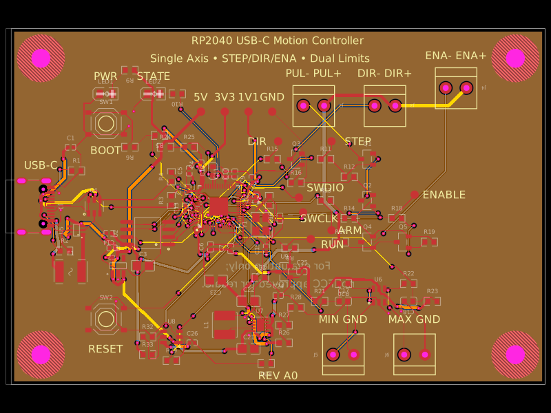 Similar packageAnasSarkiz/rp2040-usb-c-single-axis-dm542t-motion-controller--01a0e89cA USB‑C RP2040 controller board with external QSPI flash, crystal clock, regulated 3.3/1.1/5 V power, boost-converted motor-driver supply, protected USB and limit inputs, status LEDs, reset/boot switches, and AO3400A MOSFET outputs for stepper-control signals.
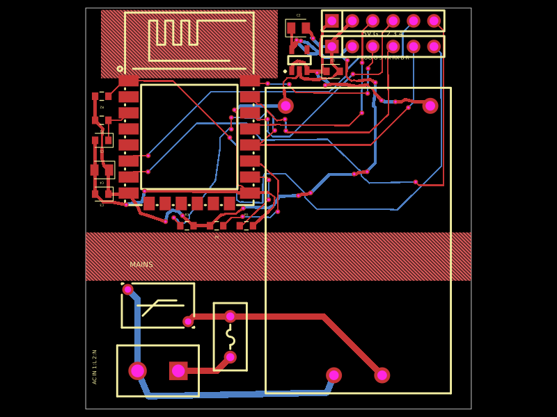 Discover something newmohan-bee/four-gang-wifi-switch-layout