mohan-bee/stm32-midi-keys
Clips rectangular ground-region geometry to fit within the board’s scaled rounded-edge outline using polygon intersection.
- Version
- 1.0.2
- License
- unset
- Stars
- 0
imports/SJ1_3523N.tsx
import type { ChipProps } from "@tscircuit/props"

const pinLabels = {
  pin1: ["pin1"],
  pin2: ["pin2"],
  pin3: ["pin3"]
} as const

export const SJ1_3523N = (props: ChipProps<typeof pinLabels>) => {
  return (
    <chip
      pinLabels={pinLabels}
      symbol={
        <symbol>
          <port name="pin3" pinNumber={3} aliases={["3"]} direction="right" schX={0.6} schY={0.2} schStemLength={0.2} />
          <port name="pin2" pinNumber={2} aliases={["2"]} direction="right" schX={0.6} schY={-0.4} schStemLength={0.2} />
          <schematicpath points={[{"x":0.4,"y":0.2},{"x":-0.08,"y":0.2},{"x":-0.12,"y":0.12},{"x":-0.16,"y":0.2}]} strokeColor="#880000" />
          <schematicpath points={[{"x":0.4,"y":-0.4},{"x":0.02,"y":-0.4},{"x":-0.02,"y":-0.32},{"x":-0.06,"y":-0.4}]} strokeColor="#880000" />
          <schematicpath points={[{"x":-0.4,"y":0.28},{"x":-0.4,"y":0.4},{"x":0.4,"y":0.4}]} strokeColor="#880000" />
          <schematicrect schX={-0.4} schY={-0.03} width={0.16} height={0.62} strokeWidth={0.02} color="#880000" />
          <port name="pin1" pinNumber={1} aliases={["1"]} direction="right" schX={0.6} schY={0.4} schStemLength={0.2} />
          <schematictext schX={0.07} schY={0.808} text="{NAME}" fontSize={0.2} anchor="bottom_center" />
        </symbol>
      }
      supplierPartNumbers={{
  "jlcpcb": [
    "C20182914"
  ]
}}
      manufacturerPartNumber="SJ1-3523N"
      footprint={<footprint>
        <hole pcbX="-0.00127mm" pcbY="-3.750056mm" diameter="1.1999976mm" />
<hole pcbX="-4.99999mm" pcbY="1.249934mm" diameter="1.1999976mm" />
<hole pcbX="4.99999mm" pcbY="1.249934mm" diameter="1.1999976mm" />
<hole pcbX="-4.99999mm" pcbY="3.750056mm" diameter="1.1999976mm" />
<hole pcbX="4.99999mm" pcbY="3.750056mm" diameter="1.1999976mm" />
<platedhole  portHints={["pin1"]} pcbX="0mm" pcbY="1.249934mm" holeWidth="1.5000224mm" holeHeight="0.7999984mm" outerWidth="2.2999954mm" outerHeight="1.499997mm" shape="pill" />
<platedhole  portHints={["pin2"]} pcbX="-4.99999mm" pcbY="-3.750056mm" holeWidth="0.7999984mm" holeHeight="1.499997mm" outerWidth="1.499997mm" outerHeight="2.2999954mm" shape="pill" />
<platedhole  portHints={["pin3"]} pcbX="4.99999mm" pcbY="-3.750056mm" holeWidth="0.7999984mm" holeHeight="1.499997mm" outerWidth="1.499997mm" outerHeight="2.2999954mm" shape="pill" />
<silkscreenpath route={[{"x":-6.001258000000007,"y":4.750562000000059},{"x":5.99871799999994,"y":4.750562000000059}]} />
<silkscreenpath route={[{"x":5.99871799999994,"y":4.750562000000059},{"x":5.99871799999994,"y":-6.2494159999999965}]} />
<silkscreenpath route={[{"x":5.99871799999994,"y":-6.2494159999999965},{"x":-6.001258000000007,"y":-6.2494159999999965}]} />
<silkscreenpath route={[{"x":-6.001258000000007,"y":4.750562000000059},{"x":-6.001258000000007,"y":-6.2494159999999965}]} />
<silkscreenpath route={[{"x":-3.0012640000001056,"y":4.750562000000059},{"x":-3.0012640000001056,"y":7.7505559999999605}]} />
<silkscreenpath route={[{"x":-3.0012640000001056,"y":7.7505559999999605},{"x":2.9987240000000384,"y":7.7505559999999605}]} />
<silkscreenpath route={[{"x":2.9987240000000384,"y":4.750562000000059},{"x":2.9987240000000384,"y":7.7505559999999605}]} />
<silkscreentext text="{NAME}" pcbX="-0.00127mm" pcbY="9.060944mm" anchorAlignment="center" fontSize="1mm" />
<fabricationnotepath route={[{"x":-3.048000000000002,"y":7.7670660000001135},{"x":-3.048000000000002,"y":4.846066000000064},{"x":2.921000000000049,"y":4.846066000000064},{"x":3.048000000000002,"y":4.846066000000064},{"x":3.048000000000002,"y":7.7670660000001135},{"x":-3.048000000000002,"y":7.7670660000001135}]} strokeWidth="0mm" isFilled hasStroke={false} />
<courtyardoutline outline={[{"x":-6.2549664000000575,"y":8.299920400000133},{"x":6.254991799999857,"y":8.299920400000133},{"x":6.254991799999857,"y":-6.500050999999985},{"x":-6.2549664000000575,"y":-6.500050999999985},{"x":-6.2549664000000575,"y":8.299920400000133}]} />
      </footprint>}
      cadModel={{
        objUrl: "https://modelcdn.tscircuit.com/easyeda_models/assets/C20182914.obj?uuid=6c333dfb5aaf4fa7911bc932745d1a18",
        stepUrl: "https://modelcdn.tscircuit.com/easyeda_models/assets/C20182914.step?uuid=6c333dfb5aaf4fa7911bc932745d1a18",
        pcbRotationOffset: 0,
        modelOriginPosition: { x: 0.0049873000000433265, y: -2.1449347000000167, z: -8.5050068 },
      }}
      {...props}
    />
  )
}
Related Packages
 More from this authormohan-bee/rp2040-crystalThis design features a 12MHz crystal oscillator with two 18pF load capacitors connected to its XIN and XOUT pins, mounted on a PCB with associated grounding traces.
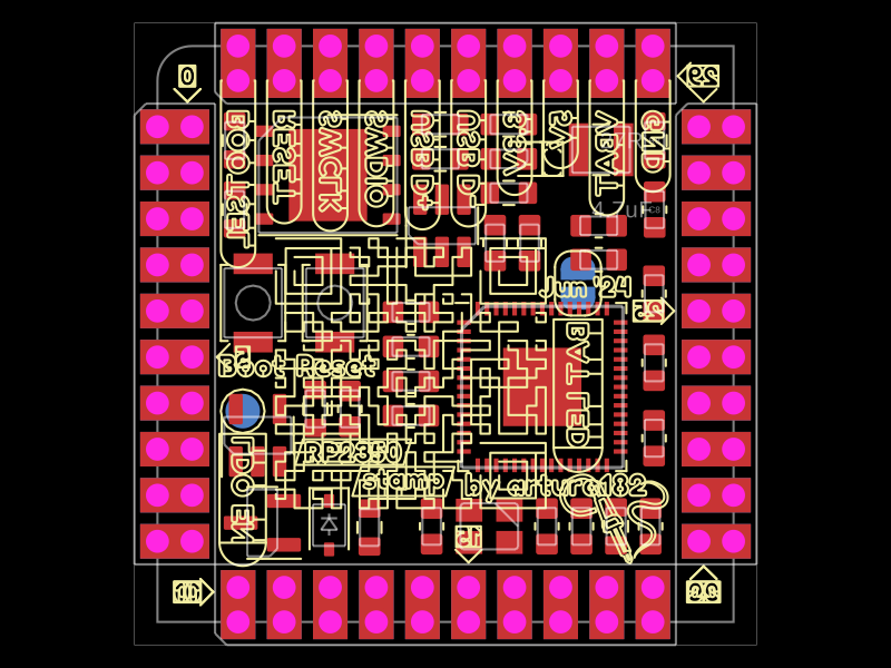 Similar packagetechmannih/imported-rp2350-stamp-boardThis code defines a detailed PCB layout with multiple layers, including the physical outline, component footprints, drilling holes, SMT pads, silkscreen markings, and courtyard outlines for component placement and board edges.
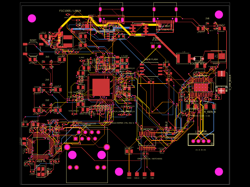 Discover something newshibosoftwaredev/f1c100s-linux-nema8-stepper-controllerRestores component part numbers and CAD models, removes test-point 3D bodies, and validates that solder paste exists only on top-side SMT pads without altering copper or DRC.