mohan-bee/gimbal-one-budget-pcb
A 4-layer STM32-based gimbal controller PCB with an onboard LSM6DS3TR-C IMU, three DRV8313 3-phase motor drivers, protected 3S battery input, 3.3 V buck regulation, and SWD/UART control interfaces.
- Version
- 0.1.0
- License
- unset
- Stars
- 0
controller.circuit.tsx
PCB

Schematic

import "tscircuit"
import { checkedRouting } from "./routing/checked-routing"
import { STM32G431CBT6 } from "./imports/STM32G431CBT6"
import { LSM6DS3TR_C } from "./imports/LSM6DS3TR_C"
import { DRV8313PWPR } from "./imports/DRV8313PWPR"
import { AP63203WU_7 } from "./imports/AP63203WU_7"
import { EEEFK1E101XP } from "./imports/EEEFK1E101XP"
import { AO4407A } from "./imports/AO4407A"
import supplierCodes from "./supplier-codes.json"

// One board, no remote IMU or separate motor-controller modules.
export const axes = [
  { name: "PITCH", x: -26, pins: [30, 31, 32], pwm: ["PA8/TIM1_CH1/AF6", "PA9/TIM1_CH2/AF6", "PA10/TIM1_CH3/AF6"], enable: 15, fault: 11 },
  { name: "ROLL", x: 0, pins: [8, 9, 10], pwm: ["PA0/TIM2_CH1/AF1", "PA1/TIM2_CH2/AF1", "PA2/TIM2_CH3/AF1"], enable: 33, fault: 12 },
  { name: "YAW", x: 26, pins: [41, 42, 16], pwm: ["PB4/TIM3_CH1/AF2", "PB5/TIM3_CH2/AF2", "PB0/TIM3_CH3/AF2"], enable: 34, fault: 13 },
] as const

const refdes: Record<string,string> = {"C_INPUT": "C1", "C_BUCK_IN": "C2", "C_BUCK_HF": "C3", "C_BST": "C4", "C_OUT1": "C5", "C_OUT2": "C6", "C_BAT_ADC": "C7", "C_VDD1": "C8", "C_VDD2": "C9", "C_VDD3": "C10", "C_MCU_BULK": "C11", "C_VBAT": "C12", "C_VDDA": "C13", "C_VREF": "C14", "C_NRST": "C15", "C_IMU_VDD": "C16", "C_IMU_BULK": "C17", "C_IMU_IO": "C18", "C_PITCH_FLY": "C19", "C_PITCH_PUMP": "C20", "C_PITCH_VM1": "C21", "C_PITCH_VM2": "C22", "C_PITCH_BULK": "C23", "C_PITCH_LDO": "C24", "C_ROLL_FLY": "C25", "C_ROLL_PUMP": "C26", "C_ROLL_VM1": "C27", "C_ROLL_VM2": "C28", "C_ROLL_BULK": "C29", "C_ROLL_LDO": "C30", "C_YAW_FLY": "C31", "C_YAW_PUMP": "C32", "C_YAW_VM1": "C33", "C_YAW_VM2": "C34", "C_YAW_BULK": "C35", "C_YAW_LDO": "C36", "R_GATE": "R1", "R_BAT_TOP": "R2", "R_BAT_BOT": "R3", "R_ANALOG": "R4", "R_NRST": "R5", "R_BOOT": "R6", "R_IMU": "R7", "R_IMU_CS": "R8", "R_PITCH_ENABLE": "R9", "R_PITCH_PD": "R10", "R_PITCH_FAULT": "R11", "R_ROLL_ENABLE": "R12", "R_ROLL_PD": "R13", "R_ROLL_FAULT": "R14", "R_YAW_ENABLE": "R15", "R_YAW_PD": "R16", "R_YAW_FAULT": "R17", "R_DRIVE_RST": "R18", "R_RST_CMD": "R19"}
const net = (name: string) => `net.${name}`
const noRefText = {silkscreenTextVisibility:"hidden" as const}
const supplier = (mpn: string) => ({jlcpcb:[(supplierCodes as Record<string,string>)[mpn]]})
const pins = (mapping: Record<number, string>) => Object.fromEntries(Object.entries(mapping).map(([p, n]) => [`pin${p}`, net(n)]))
// PCB placement stays fixed; schematic positions are generated automatically.
function location(section: string, x: number, y: number, rotation = 0) {
  return { pcbX: x, pcbY: y, pcbRotation: rotation, pcbStyle:noRefText, schSectionName: section, schSheetName: `sheet_${section}` }
}
const capacitorParts: Record<string, {mpn:string;voltage:number}> = {
  "100nF":{mpn:"CL10B104KB8NNNC",voltage:50}, "10nF":{mpn:"CL10B103KB8NNNC",voltage:50},
  "470nF":{mpn:"CC0603KRX7R7BB474",voltage:16}, "1uF":{mpn:"CL10A105KB8NNNC",voltage:50},
  "2.2uF":{mpn:"CL10A225KO8NNNC",voltage:16}, "4.7uF":{mpn:"CL21A475KAQNNNE",voltage:25},
  "10uF":{mpn:"CL21A106KAYNNNE",voltage:25}, "22uF":{mpn:"CL21A226MAYNNNE",voltage:25}
}
const resistorParts: Record<string,string> = {"100k":"RC0603FR-07100KL","220k":"RC0603FR-07220KL","27k":"RC0603FR-0727KL","10":"RC0603FR-0710RL","1k":"RC0603FR-071KL","10k":"RC0603FR-0710KL"}
function C(name: string, value: string, a: string, b: string, x: number, y: number, section: string, footprint = "0603", rotation = 0) {
  return <capacitor name={refdes[name] ?? name} capacitance={value} manufacturerPartNumber={capacitorParts[value].mpn} supplierPartNumbers={supplier(capacitorParts[value].mpn)} maxVoltageRating={capacitorParts[value].voltage} footprint={footprint} schRotation={b === "VM" ? 90 : -90} {...location(section, x, y, rotation)} connections={{ pin1: net(a), pin2: net(b) }} />
}
function R(name: string, value: string, a: string, b: string, x: number, y: number, section: string, rotation = 0) {
  return <resistor name={refdes[name] ?? name} resistance={value} manufacturerPartNumber={resistorParts[value]} supplierPartNumbers={supplier(resistorParts[value])} footprint="0603" schRotation={-90} {...location(section, x, y, rotation)} connections={{ pin1: net(a), pin2: net(b) }} />
}

export default function GimbalController({ routingDisabled = false }: { routingDisabled?: boolean } = {}) {
  const mcu: Record<number, string> = {
    1: "V3V3", 2: "DRIVE_RESET_CMD", 7: "MCU_NRST", 14: "VBAT_ADC", 18: "IMU_INT",
    19: "GND", 20: "VDDA", 21: "VDDA", 22: "UART_TX", 23: "GND", 24: "V3V3", 25: "UART_RX",
    26: "IMU_CS", 27: "IMU_SCK", 28: "IMU_MISO", 29: "IMU_MOSI", 35: "GND", 36: "V3V3",
    37: "SWDIO", 38: "SWCLK", 45: "BOOT0", 47: "GND", 48: "V3V3",
  }
  for (const axis of axes) {
    axis.pins.forEach((pin, i) => { mcu[pin] = `${axis.name}_PWM${i + 1}` })
    mcu[axis.enable] = `${axis.name}_ENABLE_CMD`
    mcu[axis.fault] = `${axis.name}_FAULT`
  }
  return <board name="CONTROLLER" width={84} height={70} layers={4} thickness={1.6}
    title="Gimbal One budget — LSM6DS3TR-C prototype" solderMaskColor="black"
    pcbSx={{"& footprint silkscreentext":{visibility:"hidden"}}}
    routingDisabled={routingDisabled} routeRemaining autorouter={{ algorithmFn: checkedRouting, allowViaInPad: false }}
    isViaInPadAllowed minTraceWidth={0.15} defaultTraceWidth={0.2} minViaHoleDiameter={0.2} minViaPadDiameter={0.45}
    schAutoLayoutEnabled schTraceAutoLabelEnabled>
    <net name="GND" isGroundNet nominalTraceWidth={0.5} />
    <net name="BAT_POS" isPowerNet nominalTraceWidth={1} />
    <net name="BAT_FUSED" isPowerNet nominalTraceWidth={1} />
    <net name="VM" isPowerNet nominalTraceWidth={1} />
    <net name="V3V3" isPowerNet nominalTraceWidth={0.35} />
    <net name="VDDA" isPowerNet nominalTraceWidth={0.25} />
    <net name="IMU_3V3" isPowerNet nominalTraceWidth={0.25} />
    {["Power", "MCU", "IMU", "PITCH", "ROLL", "YAW", "IO"].map((s, i) => <schematicsheet name={`sheet_${s}`} displayName={`Gimbal One — ${s}`} sheetSize="A4" sheetIndex={i} />)}
    {["Power", "MCU", "IMU", "PITCH", "ROLL", "YAW", "IO"].map(s => <schematicsection name={s} />)}

    <connector name="J_BAT" standard="jst_ph" pinCount={2} footprint={<footprint insertionDirection="from_above"><platedhole portHints={["pin1"]} pcbX={-1} pcbY={0} holeDiameter={0.8} outerDiameter={1.5} shape="circle" /><platedhole portHints={["pin2"]} pcbX={1} pcbY={0} holeDiameter={0.8} outerDiameter={1.5} shape="circle" /><courtyardrect width={6.5} height={5.5} /></footprint>} manufacturerPartNumber="B2B-PH-K-S(LF)(SN)" {...location("Power", -35, -25)} connections={pins({ 1: "BAT_POS", 2: "GND" })} />
    <fuse name="F1" manufacturerPartNumber="SF-1206S150-2" supplierPartNumbers={{jlcpcb:["C913209"]}} schRotation={-90} currentRating="1.5A" footprint="1206" {...location("Power", -29, -27)} connections={{ pin1: net("BAT_POS"), pin2: net("BAT_FUSED") }} />
    <AO4407A name="Q1" {...location("Power", -26, -19)} connections={pins({ 1: "VM", 2: "VM", 3: "VM", 4: "RP_GATE", 5: "BAT_FUSED", 6: "BAT_FUSED", 7: "BAT_FUSED", 8: "BAT_FUSED" })} />
    {R("R_GATE", "100k", "RP_GATE", "GND", -31, -20, "Power", 90)}
    <diode name="D_GS" schRotation={90} manufacturerPartNumber="BZT52C12" supplierPartNumbers={supplier("BZT52C12")} footprint="sod123" {...location("Power", -31, -16, 90)} connections={{ anode: net("RP_GATE"), cathode: net("VM") }} />
    <diode name="D_TVS" schRotation={90} manufacturerPartNumber="SMBJ15A" supplierPartNumbers={supplier("SMBJ15A")} footprint="smb" {...location("Power", -35, -10, 90)} connections={{ anode: net("GND"), cathode: net("VM") }} />
    <EEEFK1E101XP maxVoltageRating={25} name="C1" schRotation={-90} {...location("Power", -35, -2)} connections={{pin1:net("VM"),pin2:net("GND")}} />
    {C("C_BUCK_IN", "10uF", "VM", "GND", -24, -13, "Power", "0805", 90)}
    {C("C_BUCK_HF", "100nF", "VM", "GND", -21.5, -13, "Power", "0603", 90)}
    <AP63203WU_7 pcbStyle={noRefText} name="U_BUCK" pcbX={-24} pcbY={-8} schSectionName="Power" schSheetName="sheet_Power" connections={pins({ 1: "V3V3", 2: "VM", 3: "VM", 4: "GND", 5: "BUCK_SW", 6: "BUCK_BST" })} />
    {C("C_BST", "100nF", "BUCK_BST", "BUCK_SW", -24, -4.7, "Power")}
    <inductor name="L1" inductance="3.3uH" manufacturerPartNumber="SRN4018-3R3M" supplierPartNumbers={{jlcpcb:["C2044390"]}}
      footprint={<footprint><smtpad portHints={["pin1"]} pcbX={-1.525} pcbY={0} width={1.5} height={3.6} shape="rect" /><smtpad portHints={["pin2"]} pcbX={1.525} pcbY={0} width={1.5} height={3.6} shape="rect" /><courtyardrect width={5} height={4.5} /></footprint>}
      cadModel={{jscad:{type:"colorize",color:[0.25,0.25,0.25],shape:{type:"cuboid",size:[4,4,1.88],center:[0,0,0.94]}}}} {...location("Power", -18, -5)} connections={{ pin1: net("BUCK_SW"), pin2: net("V3V3") }} />
    {C("C_OUT1", "22uF", "V3V3", "GND", -17, -10, "Power", "0805", 90)}
    {C("C_OUT2", "22uF", "V3V3", "GND", -14, -10, "Power", "0805", 90)}
    {R("R_BAT_TOP", "220k", "VM", "VBAT_ADC", -26, -30.5, "Power")}
    {R("R_BAT_BOT", "27k", "VBAT_ADC", "GND", -22, -30.5, "Power")}
    {C("C_BAT_ADC", "100nF", "VBAT_ADC", "GND", -18, -30.5, "Power")}

    <STM32G431CBT6 pcbStyle={noRefText} name="U_MCU" pcbX={0} pcbY={-10} schWidth={3.3} schHeight={5} schSectionName="MCU" schSheetName="sheet_MCU" connections={pins(mcu)} />
    {C("C_VDD1", "100nF", "V3V3", "GND", 6.3, -11.5, "MCU", "0603", 90)}
    {C("C_VDD2", "100nF", "V3V3", "GND", -1.5, -16.3, "MCU")}
    {C("C_VDD3", "100nF", "V3V3", "GND", -6.3, -8.5, "MCU", "0603", 90)}
    {C("C_MCU_BULK", "4.7uF", "V3V3", "GND", 7.5, -7, "MCU", "0805", 90)}
    {C("C_VBAT", "100nF", "V3V3", "GND", -4.5, -18, "MCU")}
    {R("R_ANALOG", "10", "V3V3", "VDDA", -1.5, -3.7, "MCU")}
    {C("C_VDDA", "1uF", "VDDA", "GND", 1.5, -3.7, "MCU")}
    {C("C_VREF", "100nF", "VDDA", "GND", 4.5, -3.7, "MCU")}
    {R("R_NRST", "10k", "V3V3", "MCU_NRST", -7.5, -16, "MCU")}
    {C("C_NRST", "100nF", "MCU_NRST", "GND", -7.5, -19, "MCU")}
    {R("R_BOOT", "10k", "BOOT0", "GND", 1, -19, "MCU")}
    <pinheader manufacturerPartNumber="TSW-102-07-G-S" name="J_BOOT" pinCount={2} footprint="pinrow2_p2.54mm" {...location("MCU", 6, -22)} connections={pins({ 1: "BOOT0", 2: "V3V3" })} />

    <LSM6DS3TR_C pcbStyle={noRefText} name="U_IMU" pcbX={24} pcbY={-15} schWidth={2.34} schHeight={1.6} schSectionName="IMU" schSheetName="sheet_IMU" connections={pins({ 1: "IMU_MISO", 2: "GND", 3: "GND", 4: "IMU_INT", 5: "IMU_3V3", 6: "GND", 7: "GND", 8: "IMU_3V3", 12: "IMU_CS", 13: "IMU_SCK", 14: "IMU_MOSI" })} />
    {R("R_IMU", "10", "V3V3", "IMU_3V3", 18, -15, "IMU", 90)}
    {C("C_IMU_VDD", "100nF", "IMU_3V3", "GND", 27, -15, "IMU", "0603", 90)}
    {C("C_IMU_BULK", "2.2uF", "IMU_3V3", "GND", 27, -19, "IMU")}
    {C("C_IMU_IO", "10nF", "IMU_3V3", "GND", 22.5, -18, "IMU")}
    {R("R_IMU_CS", "10k", "V3V3", "IMU_CS", 23, -11, "IMU")}

    {axes.map(axis => {
      const s = axis.name, x = axis.x
      return <>
        <DRV8313PWPR pcbStyle={noRefText} name={`U_${s}`} pcbX={x} pcbY={16} schWidth={2.245} schHeight={3.4} schSectionName={s} schSheetName={`sheet_${s}`} connections={pins({ 1: `${s}_CPL`, 2: `${s}_CPH`, 3: `${s}_VCP`, 4: "VM", 5: `${s}_U`, 6: "GND", 7: "GND", 8: `${s}_V`, 9: `${s}_W`, 10: "GND", 11: "VM", 12: "GND", 13: "V3V3", 14: "GND", 15: `${s}_V3P3`, 16: "DRIVE_RESET", 17: `${s}_ENABLE`, 18: `${s}_FAULT`, 20: "GND", 22: `${s}_ENABLE`, 23: `${s}_PWM3`, 24: `${s}_ENABLE`, 25: `${s}_PWM2`, 26: `${s}_ENABLE`, 27: `${s}_PWM1`, 28: "GND", 29: "GND" })} />
        <connector name={`J_${s}`} standard="jst_ph" pinCount={3} footprint="jst3_ph" manufacturerPartNumber="B3B-PH-K-S(LF)(SN)" {...location(s, x, 29)} connections={pins({ 1: `${s}_U`, 2: `${s}_V`, 3: `${s}_W` })} />
        {["U", "V", "W"].map(p => <net name={`${s}_${p}`} nominalTraceWidth={0.6} />)}
        {C(`C_${s}_FLY`, "10nF", `${s}_CPL`, `${s}_CPH`, x - 3.8, 10.5, s, "0603")}
        {C(`C_${s}_PUMP`, "100nF", `${s}_VCP`, "VM", x - 7, 13, s, "0603", 90)}
        {C(`C_${s}_VM1`, "100nF", "VM", "GND", x - 1.2, 10.5, s, "0603", 90)}
        {C(`C_${s}_VM2`, "100nF", "VM", "GND", x + 2.4, 10.5, s, "0603", 90)}
        {C(`C_${s}_BULK`, "10uF", "VM", "GND", x - 7, 18, s, "0805", 90)}
        {C(`C_${s}_LDO`, "470nF", `${s}_V3P3`, "GND", x + 6.5, 20, s, "0603", 90)}
        {R(`R_${s}_ENABLE`, "1k", `${s}_ENABLE_CMD`, `${s}_ENABLE`, x - 5, 23, s)}
        {R(`R_${s}_PD`, "10k", `${s}_ENABLE`, "GND", x - 1, 23, s)}
        {R(`R_${s}_FAULT`, "10k", "V3V3", `${s}_FAULT`, x + 3, 23, s)}
      </>
    })}

    <pinheader manufacturerPartNumber="TSW-105-07-G-S" name="J_SWD" pinCount={5} footprint="pinrow5_p2.54mm" {...location("IO", -5, -29)} connections={pins({ 1: "V3V3", 2: "SWDIO", 3: "GND", 4: "SWCLK", 5: "MCU_NRST" })} />
    <pinheader manufacturerPartNumber="TSW-103-07-G-S" name="J_UART" pinCount={3} footprint="pinrow3_p2.54mm" {...location("IO", 17, -29)} connections={pins({ 1: "GND", 2: "UART_TX", 3: "UART_RX" })} />
    <pinheader manufacturerPartNumber="TSW-102-07-G-S" name="J_STOP" pinCount={2} footprint="pinrow2_p2.54mm" {...location("IO", 31, -29)} connections={pins({ 1: "DRIVE_RESET", 2: "GND" })} />
    {R("R_DRIVE_RST", "10k", "V3V3", "DRIVE_RESET", 12, -22, "IO")}
    {R("R_RST_CMD", "1k", "DRIVE_RESET_CMD", "DRIVE_RESET", 12, -18.5, "IO")}
    {[[-35, 4, "VM"], [-13, -24, "V3V3"], [22, -23, "GND"], [32, -18, "IMU_INT"]].map(([x, y, n]) => <testpoint pcbStyle={noRefText} doNotPlace name={`TP_${n}`} pcbX={Number(x)} pcbY={Number(y)} schSectionName="IO" schSheetName="sheet_IO" padDiameter={1.5} connections={{ pin1: net(String(n)) }} />)}
    {[[-38, -31], [38, -31], [-38, 31], [38, 31]].map(([x, y], i) => <hole name={`H${i + 1}`} pcbX={x} pcbY={y} diameter={2.7} />)}
    <fiducial name="FID1" pcbX={-38} pcbY={25} padDiameter={1} soldermaskPullback={0.5} />
    <fiducial name="FID2" pcbX={38} pcbY={-25} padDiameter={1} soldermaskPullback={0.5} />
    <silkscreentext text="GIMBAL ONE / REV B / PROTOTYPE" pcbX={0} pcbY={33} fontSize={1} />
    <silkscreentext text="3S ONLY 9.6–12.6 V" pcbX={-29} pcbY={-33} fontSize={0.8} />
    <silkscreentext text="SWD: 3V3 DIO GND CLK RST" pcbX={-5} pcbY={-33} fontSize={0.8} />
    <silkscreentext text="UART: G TX RX" pcbX={17} pcbY={-33} fontSize={0.8} />
    <silkscreentext text="STOP" pcbX={31} pcbY={-33} fontSize={0.8} />
    <silkscreentext text="IMU +X RIGHT / +Y UP" pcbX={24} pcbY={-7} fontSize={0.8} />
    {axes.map(axis => <silkscreentext text={`${axis.name} / U V W`} pcbX={axis.x} pcbY={25} fontSize={0.8} />)}
    {/* Keep top copper outside the fiducials' 0.5 mm mask pullback plus a black-mask dam. */}
    <copperpour name="GND_TOP" layer="top" connectsTo="net.GND" clearance={0.7} />
    <copperpour name="GND_INNER" layer="inner1" connectsTo="net.GND" clearance={0.25} />
    <copperpour name="GND_BOTTOM" layer="bottom" connectsTo="net.GND" clearance={0.25} />
  </board>
}
Related Packages
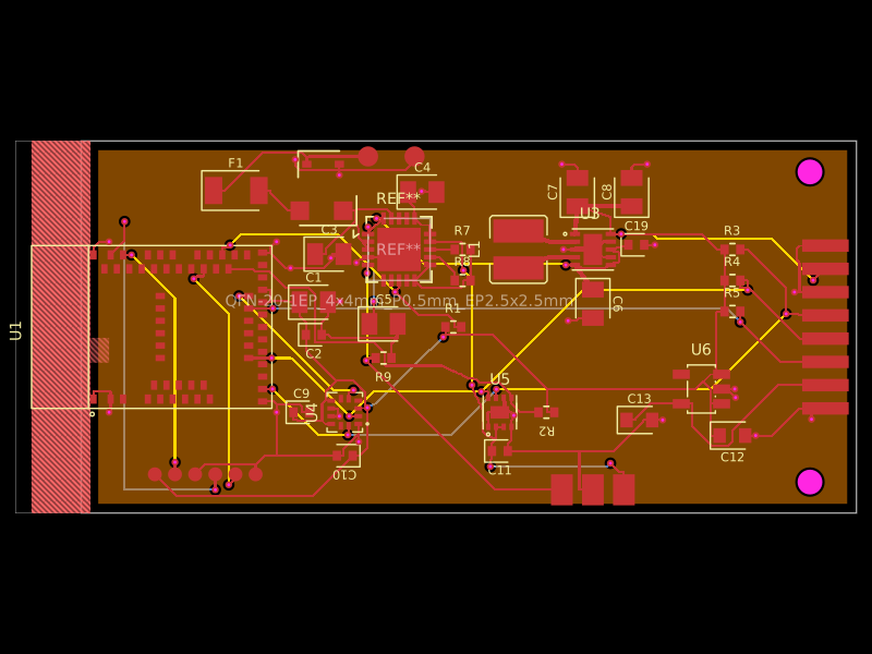 More from this authormohan-bee/fitness-bandA 4-layer BLE wearable mainboard with Li-ion charging/protection, 3.3/1.8 V power regulation, motion and battery sensing, plus a folded 2-layer flex sensor board carrying MAX30102 optical and TMP117 temperature sensors.
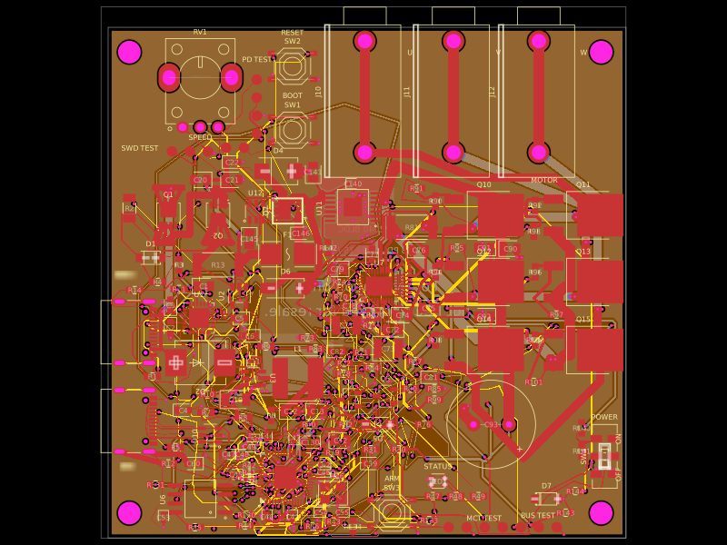 Similar packageMustafaMulla29/rp2040-bldc-motor-controller-new73×72 mm 4-layer USB‑C PD (5/9/15/20 V) RP2040 controller PCB with protected power switching, MCT8329A sensorless BLDC three-phase MOSFET bridge, USB data/programming, onboard controls, and three motor outputs feeding a 2212 motor through rigid bullet adapters.
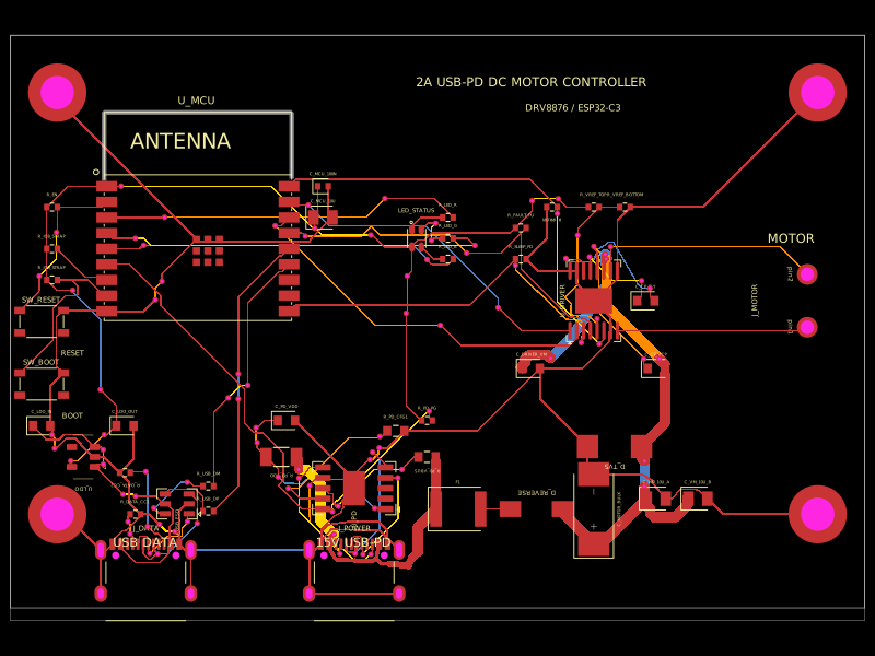 Discover something newShiboSoftwareDev/usb-pd-dc-motor-controllerUSB‑PD–powered 2A brushed-DC motor controller combining dual USB‑C ports, ESP32‑C3 control, CH224K PD negotiation, DRV8876 H‑bridge drive, protection/filtering, status RGB LED, and motor output.