mohan-bee/four-gang-wifi-switch-layout
A tscircuit package created by mohan-bee.
- Version
- 0.0.9
- License
- unset
- Stars
- 0
dist/index.cjs
'use strict';

var jsxRuntime = require('react/jsx-runtime');
var capacityAutorouter = require('@tscircuit/capacity-autorouter');
var fanoutSolver = require('@tscircuit/fanout-solver');

// Each attempt gives the entire phase to the default capacity solver.
// Configuration and validation never author or move any returned copper vertices.
function defaultCapacity(options) {
    return async (input) => {
        const srj = structuredClone(input);
        // Prior phases are obstacles, never rerouting seeds for a later width class.
        for (const trace of input.traces ?? [])
            for (let i = 0; i < trace.route.length; i++) {
                const a = trace.route[i], b = trace.route[i + 1];
                if (a.route_type === "via") {
                    const d = a.via_diameter ?? input.minViaPadDiameter ?? 0.6;
                    srj.obstacles.push({ type: "rect", center: { x: a.x, y: a.y }, width: d, height: d, layers: ["top", "bottom"], connectedTo: [trace.connection_name] });
                }
                if (!b || a.route_type !== "wire" || b.route_type !== "wire" || a.layer !== b.layer)
                    continue;
                const count = Math.max(1, Math.ceil(Math.hypot(b.x - a.x, b.y - a.y) / 0.2));
                for (let k = 0; k < count; k++) {
                    const x0 = a.x + (b.x - a.x) * k / count, y0 = a.y + (b.y - a.y) * k / count;
                    const x1 = a.x + (b.x - a.x) * (k + 1) / count, y1 = a.y + (b.y - a.y) * (k + 1) / count;
                    const width = Math.max(a.width, b.width);
                    srj.obstacles.push({ type: "rect", center: { x: (x0 + x1) / 2, y: (y0 + y1) / 2 }, width: Math.abs(x1 - x0) + width, height: Math.abs(y1 - y0) + width, layers: [a.layer], connectedTo: [trace.connection_name] });
                }
            }
        srj.traces = [];
        const barrier = input.obstacles.find(o => !o.connectedTo.length && o.width >= input.bounds.maxX - input.bounds.minX - 1e-6 && o.height >= 6);
        if (!barrier)
            throw new Error("Missing full-width isolation barrier");
        if (options.side === "below")
            srj.bounds.maxY = barrier.center.y - barrier.height / 2;
        else
            srj.bounds.minY = barrier.center.y + barrier.height / 2;
        if (options.guardPhysicalEdges) {
            // Keep compensated exterior wall geometry inside the solver's domain.
            srj.bounds.minX -= 2;
            srj.bounds.maxX += 2;
            if (options.side === "below")
                srj.bounds.minY -= 2;
            else
                srj.bounds.maxY += 2;
        }
        srj.outline = [{ x: srj.bounds.minX, y: srj.bounds.minY }, { x: srj.bounds.maxX, y: srj.bounds.minY },
            { x: srj.bounds.maxX, y: srj.bounds.maxY }, { x: srj.bounds.minX, y: srj.bounds.maxY }];
        // Obstacles outside the phase domain cannot be reached; the isolation band
        // is enforced by the domain boundary and checked against the original SRJ.
        srj.obstacles = srj.obstacles.filter(o => o.center.x + o.width / 2 > srj.bounds.minX && o.center.x - o.width / 2 < srj.bounds.maxX &&
            o.center.y + o.height / 2 > srj.bounds.minY && o.center.y - o.height / 2 < srj.bounds.maxY);
        const requested = input.minTraceToPadEdgeClearance ?? 0.2;
        // Core carries the board's smaller nominal width into wider power phases.
        srj.nominalTraceWidth = Math.max(input.nominalTraceWidth ?? 0, input.minTraceWidth, ...input.connections.map(c => c.nominalTraceWidth ?? c.width ?? 0));
        srj.defaultObstacleMargin = requested >= 1 ? requested : requested + 0.05;
        // Physical edges and the artificial isolation boundary have separate margins.
        const inset = (input.minBoardEdgeClearance ?? 0.5) + 0.01 - srj.defaultObstacleMargin;
        const b = input.bounds, cx = (b.minX + b.maxX) / 2, cy = (b.minY + b.maxY) / 2;
        srj.obstacles.push({ type: "rect", center: { x: b.minX - 10 + inset, y: cy }, width: 20, height: b.maxY - b.minY + 40, layers: ["top", "bottom"], connectedTo: [] }, { type: "rect", center: { x: b.maxX + 10 - inset, y: cy }, width: 20, height: b.maxY - b.minY + 40, layers: ["top", "bottom"], connectedTo: [] }, { type: "rect", center: { x: cx, y: b.minY - 10 + inset }, width: b.maxX - b.minX + 40, height: 20, layers: ["top", "bottom"], connectedTo: [] }, { type: "rect", center: { x: cx, y: b.maxY + 10 - inset }, width: b.maxX - b.minX + 40, height: 20, layers: ["top", "bottom"], connectedTo: [] });
        srj.minBoardEdgeClearance = 0.205;
        if (!input.allowViaInPad && !options.layer) {
            const names = new Set(input.connections.filter(c => (c.nominalTraceWidth ?? c.width ?? 0) >= 0.35).map(c => c.name));
            // Default capacity may otherwise drop a via directly in its own SMD pad.
            // An opposite-layer guard requires a top-side escape before changing layers.
            for (const pad of input.obstacles) {
                if (!pad.circuitJsonMetadata?.pcb_smtpad_id || pad.layers.length !== 1 || !pad.connectedTo.some(id => names.has(id)))
                    continue;
                srj.obstacles.push({ type: "rect", obstacleId: `via_guard_${pad.circuitJsonMetadata.pcb_smtpad_id}`,
                    center: { ...pad.center }, width: pad.width, height: pad.height, layers: [pad.layers[0] === "top" ? "bottom" : "top"], connectedTo: [] });
            }
        }
        srj.minViaPadDiameter = srj.min_via_pad_diameter = srj.minViaDiameter = 0.6 + 2 * (options.viaPlanningMargin ?? 0);
        srj.minViaHoleDiameter = srj.min_via_hole_diameter = 0.3;
        if (options.layer) {
            const layer = options.layer;
            srj.layerCount = 1;
            srj.obstacles = srj.obstacles.filter(o => o.layers.includes(layer)).map(o => ({ ...o, layers: ["top"] }));
            srj.connections = srj.connections.map(c => ({ ...c, pointsToConnect: c.pointsToConnect.map(({ layer: _, layers: __, ...p }) => ({ ...p, layer: "top" })) }));
            srj.traces = [];
        }
        const configurations = [{}, { maxNodeDimension: 8 }, { maxNodeDimension: 5 }];
        let attempt = 0;
        const createSolver = () => new capacityAutorouter.AutoroutingPipelineSolver(structuredClone(srj), { effort: 1, ...configurations[attempt] });
        let solver = createSolver();
        const step = () => {
            // The current simplifier loses wide-trace pad clearance. Keep the default
            // high-density paths for opted-in phases, with all later checks retained.
            if (options.preserveHighDensityPaths) {
                if (solver.traceSimplificationSolver)
                    solver.traceSimplificationSolver.MAX_SIMPLIFICATION_PIPELINE_LOOPS = 0;
                if (solver.mutatedPreloadedTraceSimplificationSolver)
                    solver.mutatedPreloadedTraceSimplificationSolver.MAX_SIMPLIFICATION_PIPELINE_LOOPS = 0;
            }
            solver.step();
        };
        const listeners = new Map();
        let routing = false, stopped = false, result;
        const emit = (type, event) => { for (const listener of listeners.get(type) ?? [])
            listener({ type, ...event }); };
        const finish = () => {
            if (!solver.solved)
                throw new Error(`${solver.getCurrentPhase()}: ${solver.error ?? "Default capacity autorouter failed"}`);
            const output = solver.getOutputSimpleRouteJson();
            // Reserve extra via space during routing, then use the board's physical
            // 0.6/0.3 mm via. Solver-generated centerlines are never edited.
            if (options.viaPlanningMargin)
                for (const trace of output.traces ?? [])
                    for (const point of trace.route)
                        if (point.route_type === "via") {
                            point.via_diameter = 0.6;
                            point.via_hole_diameter = 0.3;
                        }
            if (options.layer)
                for (const trace of output.traces ?? [])
                    for (const point of trace.route) {
                        if (point.route_type !== "wire")
                            throw new Error("Unexpected via in single-layer mains phase");
                        point.layer = options.layer;
                    }
            const problems = validateCandidate(input, output.traces ?? []);
            if (problems.length)
                throw new Error(`Capacity candidate rejected: ${problems.slice(0, 3).join("; ")}`);
            result = { ...input, traces: output.traces };
            emit("complete", { traces: output.traces });
            return output.traces ?? [];
        };
        return {
            input, get isRouting() { return routing; },
            on(type, listener) { listeners.set(type, [...(listeners.get(type) ?? []), listener]); },
            stop() { stopped = true; }, getOutputSimpleRouteJson() { return result; },
            solveSync() { while (!solver.solved && !solver.failed)
                step(); return finish(); },
            start() {
                console.log(`[${options.name}] ${solver.getSolverName()} FULL PHASE: ${srj.connections.length} connections; planning margin=${srj.defaultObstacleMargin}; preserve HD paths=${!!options.preserveHighDensityPaths}`);
                routing = true;
                const started = Date.now();
                const run = () => {
                    try {
                        for (let i = 0; i < 256 && !solver.solved && !solver.failed; i++)
                            step();
                        if (stopped || Date.now() - started > 240000)
                            throw new Error("Default capacity phase stopped or timed out");
                        if (solver.solved || solver.failed) {
                            routing = false;
                            finish();
                            return;
                        }
                        emit("progress", { progress: solver.computeProgress(), steps: solver.iterations });
                        setTimeout(run, 0);
                    }
                    catch (error) {
                        if (!stopped && attempt + 1 < configurations.length && Date.now() - started < 220000) {
                            console.warn(`[${options.name}] rejected configuration ${attempt}: ${error}`);
                            attempt++;
                            solver = createSolver();
                            console.log(`[${options.name}] retrying FULL PHASE with default capacity, mesh configuration ${attempt}`);
                            setTimeout(run, 0);
                        }
                        else {
                            routing = false;
                            emit("error", { error });
                        }
                    }
                };
                setTimeout(run, 0);
            },
        };
    };
}
function validateCandidate(input, newTraces) {
    const normalize = (traces) => structuredClone(traces).map(t => {
        for (let i = 1; i < t.route.length - 1; i++) {
            const p = t.route[i], a = t.route[i - 1], b = t.route[i + 1];
            if (p.route_type === "via" && a.route_type === "wire" && b.route_type === "wire" && a.layer !== b.layer) {
                p.from_layer = a.layer;
                p.to_layer = b.layer;
            }
        }
        return t;
    });
    const previous = normalize(input.traces ?? []), current = normalize(newTraces);
    const names = new Set(input.connections.map(c => c.name));
    const connections = [...input.connections, ...[...new Set(previous.map(t => t.connection_name))].filter(n => !names.has(n)).map(name => ({ name, pointsToConnect: [] }))];
    const obstacles = input.obstacles.map(o => (o.type === "oval" && Math.abs(o.width - o.height) < 1e-6 ? { ...o, shape: "circle" } : o));
    const scene = { ...input, connections, traces: [...previous, ...current] };
    const copper = { ...scene, obstacles: obstacles.filter(o => o.connectedTo.length) };
    const errors = fanoutSolver.validateRoutedCopperDrc({ inputSrj: copper, routedSrj: copper, clearance: Math.min(input.minTraceToPadEdgeClearance ?? 0.2, 0.2), allowBlindAndBuriedVias: false }).issues.map(i => i.message);
    // Every net in a mains phase is checked against prior copper at the mains rule.
    if ((input.minTraceToPadEdgeClearance ?? 0.2) >= 1) {
        const hv = copper;
        errors.push(...fanoutSolver.validateRoutedCopperDrc({ inputSrj: { ...hv, obstacles: copper.obstacles }, routedSrj: hv, clearance: input.minTraceToPadEdgeClearance, allowBlindAndBuriedVias: false }).issues.map(i => i.message));
    }
    const keepouts = { ...scene, traces: current, obstacles: obstacles.filter(o => !o.connectedTo.length) };
    errors.push(...fanoutSolver.validateRoutedCopperDrc({ inputSrj: keepouts, routedSrj: keepouts, clearance: 0.2, allowBlindAndBuriedVias: false }).issues.map(i => i.message));
    for (const trace of current)
        for (let index = 0; index < trace.route.length; index++) {
            const p = trace.route[index], next = trace.route[index + 1];
            const minimum = input.minTraceWidth;
            if (p.route_type === "wire" && next?.route_type === "wire" && p.layer === next.layer && Math.hypot(next.x - p.x, next.y - p.y) > 1e-9 && p.width + 1e-5 < minimum)
                errors.push(`width ${p.width} below configured minimum ${minimum} on ${trace.connection_name}`);
            if (p.route_type !== "via")
                continue;
            const radius = (p.via_hole_diameter ?? 0.3) / 2;
            for (const pad of obstacles.filter(o => o.circuitJsonMetadata?.pcb_smtpad_id || o.circuitJsonMetadata?.pcb_plated_hole_id)) {
                const dx = Math.max(0, Math.abs(p.x - pad.center.x) - pad.width / 2), dy = Math.max(0, Math.abs(p.y - pad.center.y) - pad.height / 2);
                const distance = pad.shape === "circle" ? Math.max(0, Math.hypot(p.x - pad.center.x, p.y - pad.center.y) - pad.width / 2) : Math.hypot(dx, dy);
                if (distance + 1e-6 < radius)
                    errors.push(`via drill overlaps ${pad.circuitJsonMetadata?.pcb_smtpad_id ?? pad.circuitJsonMetadata?.pcb_plated_hole_id}`);
            }
        }
    return errors;
}

// 48 x 50 mm controller/power PCB. Draft routing; isolated 5V supply branch only.
// JLC footprints retain EasyEDA pad numbering, including the ESP-12F's 9=GND.
function ControllerBoard() {
    return (jsxRuntime.jsxs("board", { width: 48, height: 50, layers: 2, thickness: 1.6, doubleSidedAssembly: false, title: "4 gang WiFi - controller and power", autorouter: "auto_local", routeRemaining: false, autorouterVersion: "beta_pipeline9", minViaPadDiameter: 0.6, minViaHoleDiameter: 0.3, minTraceWidth: 0.2, minTraceToPadEdgeClearance: 0.2, minViaEdgeToPadEdgeClearance: 0.2, minPadEdgeToPadEdgeClearance: 0.2, minViaHoleEdgeToViaHoleEdgeClearance: 0.2, minBoardEdgeClearance: 0.5, schAutoLayoutEnabled: true, children: [jsxRuntime.jsx("net", { name: "AC_L", nominalTraceWidth: 0.8, routingPhaseIndex: 1 }), jsxRuntime.jsx("net", { name: "AC_L_FUSED", nominalTraceWidth: 0.8, routingPhaseIndex: 1 }), jsxRuntime.jsx("net", { name: "AC_N", nominalTraceWidth: 0.8, routingPhaseIndex: 0 }), jsxRuntime.jsx("net", { name: "V5", nominalTraceWidth: 0.4, routingPhaseIndex: 2 }), jsxRuntime.jsx("net", { name: "GND", nominalTraceWidth: 0.4, routingPhaseIndex: 2 }), jsxRuntime.jsx("net", { name: "V3V3", nominalTraceWidth: 0.4, routingPhaseIndex: 2 }), ["EN", "RST", "BOOT", "STRAP2", "STRAP15", "CH1", "CH2", "CH3", "CH4", "TX", "RX"].map(name => jsxRuntime.jsx("net", { name: name, nominalTraceWidth: 0.2, routingPhaseIndex: 2 }, name)), jsxRuntime.jsx("autoroutingphase", { name: "SUPPLY_NEUTRAL", phaseIndex: 0, algorithmFn: defaultCapacity({ name: "controller-SUPPLY_NEUTRAL", side: "below", layer: "bottom", guardPhysicalEdges: true }), minTraceWidth: 0.8, minTraceToPadEdgeClearance: 1.5, minViaEdgeToPadEdgeClearance: 1.5, minBoardEdgeClearance: 0.75 }), jsxRuntime.jsx("autoroutingphase", { name: "MAINS_LIVE", phaseIndex: 1, algorithmFn: defaultCapacity({ name: "controller-MAINS_LIVE", side: "below", layer: "top" }), minTraceWidth: 0.8, minTraceToPadEdgeClearance: 1.5, minViaEdgeToPadEdgeClearance: 1.5, minBoardEdgeClearance: 0.75 }), jsxRuntime.jsx("autoroutingphase", { name: "JOINT_LV", phaseIndex: 2, minTraceWidth: 0.2, algorithmFn: defaultCapacity({ name: "controller-joint-lv", side: "above", viaPlanningMargin: 0.12 }) }), jsxRuntime.jsx("chip", { layer: "top", name: "U1", manufacturerPartNumber: "ESP-12F(ESP8266MOD)", footprint: "jlcpcb:C82891", supplierPartNumbers: { jlcpcb: ["C82891"] }, pcbX: -11.1, pcbY: 8.2, pcbRotation: -90, pinLabels: { pin1: "RST", pin2: "ADC", pin3: "EN", pin4: "GPIO16", pin5: "GPIO14", pin6: "GPIO12", pin7: "GPIO13", pin8: "V3V3", pin9: "GND", pin10: "GPIO15", pin11: "GPIO2", pin12: "GPIO0", pin13: "GPIO4", pin14: "GPIO5", pin15: "RX", pin16: "TX", pin17: "CS0", pin18: "MISO", pin19: "GPIO9", pin20: "GPIO10", pin21: "MOSI", pin22: "SCLK" }, pinAttributes: { V3V3: { requiresPower: true, requiresVoltage: 3.3 }, GND: { requiresGround: true }, CS0: { doNotConnect: true }, MISO: { doNotConnect: true }, GPIO9: { doNotConnect: true }, GPIO10: { doNotConnect: true }, MOSI: { doNotConnect: true }, SCLK: { doNotConnect: true } }, connections: { V3V3: "net.V3V3", GND: "net.GND", EN: "net.EN", RST: "net.RST", GPIO0: "net.BOOT", GPIO2: "net.STRAP2", GPIO15: "net.STRAP15", GPIO4: "net.CH1", GPIO5: "net.CH2", GPIO12: "net.CH3", GPIO13: "net.CH4", TX: "net.TX", RX: "net.RX" } }), jsxRuntime.jsx("chip", { layer: "top", doNotPlace: true, name: "PS1", manufacturerPartNumber: "HLK-5M05", footprint: "jlcpcb:C209907", supplierPartNumbers: { jlcpcb: ["C209907"] }, pcbX: 9.9, pcbY: -4, pcbRotation: 90, pinLabels: { pin1: "AC_N", pin2: "AC_L", pin3: "GND", pin4: "V5" }, pinAttributes: { V5: { providesPower: true, providesVoltage: 5 }, GND: { providesGround: true } }, connections: { AC_N: "net.AC_N", AC_L: "net.AC_L_FUSED", GND: "net.GND", V5: "net.V5" } }), jsxRuntime.jsx("chip", { layer: "top", name: "U2", manufacturerPartNumber: "AP2112K-3.3TRG1", footprint: "jlcpcb:C51118", supplierPartNumbers: { jlcpcb: ["C51118"] }, pcbX: 2.6, pcbY: 18.5, pinLabels: { pin1: "VIN", pin2: "GND", pin3: "EN", pin4: "NC", pin5: "VOUT" }, pinAttributes: { VIN: { requiresPower: true, requiresVoltage: 5 }, GND: { requiresGround: true }, VOUT: { providesPower: true, providesVoltage: 3.3 }, NC: { doNotConnect: true } }, connections: { VIN: "net.V5", GND: "net.GND", EN: "net.V5", VOUT: "net.V3V3" } }), jsxRuntime.jsx("capacitor", { name: "C1", capacitance: "10uF", voltageRating: 10, footprint: "0603", supplierPartNumbers: { jlcpcb: ["C19702"] }, pcbX: 6.8, pcbY: 17.1, layer: "top", connections: { pin1: "net.V5", pin2: "net.GND" } }), jsxRuntime.jsx("capacitor", { name: "C2", capacitance: "22uF", voltageRating: 25, footprint: "0805", supplierPartNumbers: { jlcpcb: ["C45783"] }, pcbX: 2.5, pcbY: 22.5, layer: "top", connections: { pin1: "net.V3V3", pin2: "net.GND" } }), jsxRuntime.jsx("capacitor", { name: "C3", capacitance: "100nF", voltageRating: 50, footprint: "0603", supplierPartNumbers: { jlcpcb: ["C14663"] }, pcbX: -22, pcbY: 1.8, pcbRotation: 180, layer: "top", connections: { pin1: "net.V3V3", pin2: "net.GND" } }), jsxRuntime.jsx("capacitor", { name: "C4", capacitance: "22uF", voltageRating: 25, footprint: "0805", supplierPartNumbers: { jlcpcb: ["C45783"] }, pcbX: -22, pcbY: 4.8, pcbRotation: 180, layer: "top", connections: { pin1: "net.V3V3", pin2: "net.GND" } }), jsxRuntime.jsx("capacitor", { name: "C5", capacitance: "100nF", voltageRating: 50, footprint: "0603", supplierPartNumbers: { jlcpcb: ["C14663"] }, pcbX: -22, pcbY: 8.5, layer: "top", pcbRotation: 180, connections: { pin1: "net.EN", pin2: "net.GND" } }), [
                { name: "R1", x: -22, y: 11, net: "EN", pull: "V3V3", rotation: 180 },
                { name: "R2", x: -22, y: 14, net: "RST", pull: "V3V3", rotation: 180 },
                { name: "R3", x: -11.4, y: -2.15, net: "BOOT", pull: "V3V3", rotation: 0 },
                { name: "R4", x: -7.7, y: -2.15, net: "STRAP2", pull: "V3V3", rotation: 180 },
                { name: "R5", x: -4, y: -2.15, net: "STRAP15", pull: "GND", rotation: 0 },
            ].map(r => jsxRuntime.jsx("resistor", { name: r.name, resistance: "10k", footprint: "0603", supplierPartNumbers: { jlcpcb: ["C25804"] }, pcbX: r.x, pcbY: r.y, layer: "top", pcbRotation: r.rotation, connections: { pin1: `net.${r.net}`, pin2: `net.${r.pull}` } }, r.name)), jsxRuntime.jsx("pinheader", { pinCount: 2, gender: "male", layer: "top", doNotPlace: true, name: "J_AC", manufacturerPartNumber: "PZ508V-11-02P-H25", footprint: "jlcpcb:C25170858", supplierPartNumbers: { jlcpcb: ["C25170858"] }, pcbX: -15, pcbY: -20.25, pcbRotation: 180, pinLabels: { pin1: "L", pin2: "N" }, connections: { L: "net.AC_L", N: "net.AC_N" }, children: jsxRuntime.jsx("courtyardrect", { pcbX: 0, pcbY: 0, width: 10.66, height: 6.85 }) }), jsxRuntime.jsx("chip", { layer: "top", doNotPlace: true, name: "F1", manufacturerPartNumber: "2009T500mA250V", footprint: "jlcpcb:C529783", supplierPartNumbers: { jlcpcb: ["C529783"] }, pcbX: -6, pcbY: -16, pcbRotation: 90, pinLabels: { pin1: "IN", pin2: "OUT" }, connections: { IN: "net.AC_L", OUT: "net.AC_L_FUSED" } }), jsxRuntime.jsx("chip", { layer: "top", doNotPlace: true, name: "RV1", manufacturerPartNumber: "10D561K", footprint: "jlcpcb:C2839517", supplierPartNumbers: { jlcpcb: ["C2839517"] }, pcbX: -15, pcbY: -12.1, pcbRotation: 180, pinLabels: { pin1: "L", pin2: "N" }, connections: { L: "net.AC_L_FUSED", N: "net.AC_N" } }), jsxRuntime.jsx("pinheader", { pinCount: 6, gender: "male", layer: "top", doNotPlace: true, name: "J_LINK", manufacturerPartNumber: "17-0020-002", footprint: "jlcpcb:C6800644", supplierPartNumbers: { jlcpcb: ["C6800644"] }, pcbX: 13, pcbY: 23.4, pinLabels: { pin1: "V5", pin2: "GND", pin3: "CH1", pin4: "CH2", pin5: "CH3", pin6: "CH4" }, connections: { V5: "net.V5", GND: "net.GND", CH1: "net.CH1", CH2: "net.CH2", CH3: "net.CH3", CH4: "net.CH4" } }), jsxRuntime.jsx("pinheader", { pinCount: 6, gender: "male", layer: "top", doNotPlace: true, name: "J_PROG", manufacturerPartNumber: "17-0020-002", footprint: "jlcpcb:C6800644", supplierPartNumbers: { jlcpcb: ["C6800644"] }, pcbX: 13, pcbY: 20.2, pinLabels: { pin1: "GND", pin2: "V3V3", pin3: "TX", pin4: "RX", pin5: "BOOT", pin6: "RST" }, connections: { GND: "net.GND", V3V3: "net.V3V3", TX: "net.TX", RX: "net.RX", BOOT: "net.BOOT", RST: "net.RST" } }), jsxRuntime.jsx("keepout", { shape: "rect", pcbX: 0, pcbY: -6, width: 48, height: 6, layers: ["top", "bottom"], excludeRefs: [".PS1"] }), jsxRuntime.jsx("keepout", { shape: "rect", pcbX: -11.1, pcbY: 20.5, width: 22, height: 8.5, layers: ["top", "bottom"], excludeRefs: [".U1"] }), jsxRuntime.jsx("silkscreentext", { text: "5V G 1 2 3 4", pcbX: 13, pcbY: 21.8, fontSize: 0.8 }), jsxRuntime.jsx("silkscreentext", { text: "PROG G 3 TX RX B R", pcbX: 13, pcbY: 18.8, fontSize: 0.65 }), jsxRuntime.jsx("silkscreentext", { text: "AC IN 1:L 2:N", pcbX: -22.9, pcbY: -19.8, pcbRotation: 90, fontSize: 0.65 }), jsxRuntime.jsx("silkscreentext", { text: "MAINS", pcbX: -17, pcbY: -7, fontSize: 0.9 })] }));
}

module.exports = ControllerBoard;
Related Packages
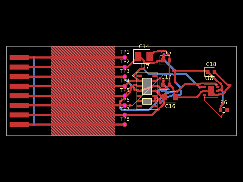 More from this authormohan-bee/fitness-band-sensor-flexA flexible dual-sensor PCB integrating a MAX30102 optical PPG/heart-rate sensor and TMP117 digital skin-temperature sensor, with I²C, power regulation, decoupling capacitors, interrupt pull-up, flex-tail connector, test points, and mechanical stiffeners/bend support.
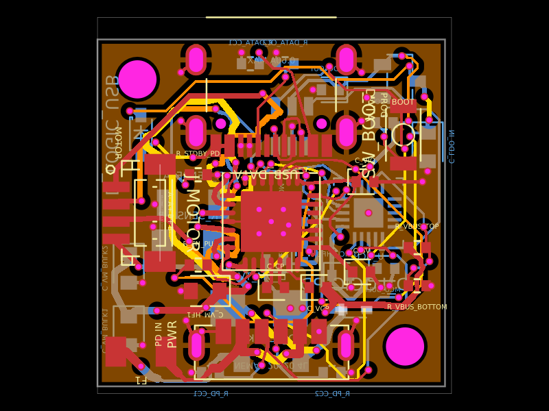 Discover something newShiboSoftwareDev/nema8-20mm-usbc-pd-controllerA 20×20 mm four-layer USB‑C PD stepper motor controller PCB using a CH32X035 MCU, TMC2209 driver, protected power inputs, USB data/boot interface, 3.3 V regulation, ESD/TVS protection, current-sense circuitry, and NEMA‑8 motor outputs.