mohan-bee/fitness-band
A 4-layer BLE wearable mainboard with Li-ion charging/protection, 3.3/1.8 V power regulation, motion and battery sensing, plus a folded 2-layer flex sensor board carrying MAX30102 optical and TMP117 temperature sensors.
- Version
- 0.0.2
- License
- unset
- Stars
- 0
validation/site-build.log
Building 4 file(s)...
Building dist/autorouter-debug/board.source-and-pcb.circuit.json...
Generating circuit JSON...
Circuit JSON written to dist/dist/autorouter-debug/board.source-and-pcb/circuit.json
The "J" prefix is being used with a <chip />, try using it with a <connector /> or <jumper />
The "J" prefix is being used with a <chip />, try using it with a <connector /> or <jumper />
The "J" prefix is being used with a <chip />, try using it with a <connector /> or <jumper />
The "J" prefix is being used with a <chip />, try using it with a <connector /> or <jumper />
Port VBUS on U1 is missing a trace
J_SWD has no pin with requires_power=true
J_SWD has no pin with requires_ground=true
All pins on J_SWD are underspecified (no pinAttributes set)
U2 has no pin with requires_power=true
U2 has no pin with requires_ground=true
All pins on U2 are underspecified (no pinAttributes set)
J_BAT has no pin with requires_power=true
J_BAT has no pin with requires_ground=true
All pins on J_BAT are underspecified (no pinAttributes set)
J_CHG has no pin with requires_power=true
J_CHG has no pin with requires_ground=true
All pins on J_CHG are underspecified (no pinAttributes set)
U6 has no pin with requires_power=true
J_FLEX has no pin with requires_power=true
J_FLEX has no pin with requires_ground=true
All pins on J_FLEX are underspecified (no pinAttributes set)
No <schematicsheet> was found. Add a <schematicsheet> to define the schematic drawing area.
J_SWD has no courtyard
J_BAT has no courtyard
J_CHG has no courtyard
J_FLEX has no courtyard
L1 may not have availability from jlcpcb (C501946).
<capacitor#170 name=".C2" /> footprint "0402" does not match supplier footprint jlcpcb:C1525 (copper IoU 0.7249).
<resistor#314 name=".R1" /> footprint "0402" does not match supplier footprint jlcpcb:C25744 (copper IoU 0.7741).
<resistor#327 name=".R2" /> footprint "0402" does not match supplier footprint jlcpcb:C25744 (copper IoU 0.7741).
<capacitor#254 name=".C9" /> footprint "0402" does not match supplier footprint jlcpcb:C1525 (copper IoU 0.7249).
<resistor#340 name=".R3" /> footprint "0402" does not match supplier footprint jlcpcb:C25900 (copper IoU 0.7741).
<capacitor#278 name=".C11" /> footprint "0402" does not match supplier footprint jlcpcb:C1525 (copper IoU 0.7249).
<capacitor#266 name=".C10" /> footprint "0402" does not match supplier footprint jlcpcb:C1525 (copper IoU 0.7249).
<resistor#366 name=".R5" /> footprint "0402" does not match supplier footprint jlcpcb:C25900 (copper IoU 0.7741).
<resistor#353 name=".R4" /> footprint "0402" does not match supplier footprint jlcpcb:C25900 (copper IoU 0.7741).
U1 may not have availability from jlcpcb (C5118826).
Building index.circuit.tsx...
Generating circuit JSON...
Each child in a list should have a unique "key" prop.

Check the render method of `MainBoard`. It was passed a child from FlexConnections. See https://react.dev/link/warning-keys for more information.
Each child in a list should have a unique "key" prop.

Check the render method of `board`. It was passed a child from MainBoard. See https://react.dev/link/warning-keys for more information.
Each child in a list should have a unique "key" prop.

Check the render method of `FlexLanding`. See https://react.dev/link/warning-keys for more information.
Autorouting <board#506 /> phase 1/1 failed start: connections=22, obstacles=369, previous_traces=0, router=tscircuit, solver=AutoroutingPipelineSolver9_PreloadedTraceGraph, cache=miss, cache_id=12cad7cd/42f09225
  connections: R7.pin1 to U2.PROG1, R8.pin1 to U2.PROG3, net.GND, net.V3V3, net.V1V8, net.VBAT, net.VSYS, net.CHG_5V, net.DOCK_5V, net.FUSED_5V, net.SDA, net.SCL, net.PPG_INT, net.MOTION_INT, net.CHG_INT, net.FG_INT, net.SWDIO, net.SWDCLK, net.RESET, net.BAT_NTC, net.SW1, net.SW2
  phase 1/1 error after 2.3s: Static reachability precheck failed: 1 route(s) have no legal path under the current reservation and start-region rules net.V3V3_mst9 (internal element->internal element) (capacity-autorouter@0.0.988)
Async effect error in PcbTraceRender "autorouting":
AutorouterError: Static reachability precheck failed: 1 route(s) have no legal path under the current reservation and start-region rules source_net_1_mst9 (pcb_port_127->pcb_port_170) (capacity-autorouter@0.0.988)
    at runCycleAndQueueNextCycle (/Users/mohan/Documents/Codex/2026-10-21/screenless-fitness-tracker-custom-pcb-plan/outputs/fitness-band/node_modules/@tscircuit/core/dist/index.js:139820:24)
    at <anonymous> (/Users/mohan/Documents/Codex/2026-10-21/screenless-fitness-tracker-custom-pcb-plan/outputs/fitness-band/node_modules/@tscircuit/core/dist/index.js:139855:27)
Circuit JSON written to dist/index/circuit.json
The "J" prefix is being used with a <chip />, try using it with a <connector /> or <jumper />
The "J" prefix is being used with a <chip />, try using it with a <connector /> or <jumper />
The "J" prefix is being used with a <chip />, try using it with a <connector /> or <jumper />
The "J" prefix is being used with a <chip />, try using it with a <connector /> or <jumper />
<trace#1339(from:.R7 > .pin1 to:.U2 > .PROG1) /> is missing a name. Add a name prop to make the trace easier to identify.
<trace#1341(from:.R8 > .pin1 to:.U2 > .PROG3) /> is missing a name. Add a name prop to make the trace easier to identify.
Port VBUS on U1 is missing a trace
J_SWD has no pin with requires_power=true
J_SWD has no pin with requires_ground=true
All pins on J_SWD are underspecified (no pinAttributes set)
U2 has no pin with requires_power=true
U2 has no pin with requires_ground=true
All pins on U2 are underspecified (no pinAttributes set)
J_BAT has no pin with requires_power=true
J_BAT has no pin with requires_ground=true
All pins on J_BAT are underspecified (no pinAttributes set)
J_CHG has no pin with requires_power=true
J_CHG has no pin with requires_ground=true
All pins on J_CHG are underspecified (no pinAttributes set)
D1 has no pin with requires_power=true
D1 has no pin with requires_ground=true
All pins on D1 are underspecified (no pinAttributes set)
D2 has no pin with requires_power=true
D2 has no pin with requires_ground=true
All pins on D2 are underspecified (no pinAttributes set)
U6 has no pin with requires_power=true
J_FLEX has no pin with requires_power=true
J_FLEX has no pin with requires_ground=true
All pins on J_FLEX are underspecified (no pinAttributes set)
No <schematicsheet> was found. Add a <schematicsheet> to define the schematic drawing area.
J_FLEX has no courtyard
Trace [.U3 > .VOUT to .C7 > .pin1] is routed thinner than requested (requested: 0.3mm, actual: 0.15mm).
Trace [.C7 > .pin1 to .C8 > .pin1] is routed thinner than requested (requested: 0.3mm, actual: 0.15mm).
L1 may not have availability from jlcpcb (C5350399).
<resistor#409 name=".R1" /> footprint "0402" does not match supplier footprint jlcpcb:C25744 (copper IoU 0.7741).
<resistor#435 name=".R3" /> footprint "0402" does not match supplier footprint jlcpcb:C25900 (copper IoU 0.7741).
<resistor#448 name=".R4" /> footprint "0402" does not match supplier footprint jlcpcb:C25900 (copper IoU 0.7741).
<capacitor#253 name=".C2" /> footprint "0402" does not match supplier footprint jlcpcb:C1525 (copper IoU 0.7249).
<resistor#461 name=".R5" /> footprint "0402" does not match supplier footprint jlcpcb:C25900 (copper IoU 0.7741).
<capacitor#397 name=".C19" /> footprint "0402" does not match supplier footprint jlcpcb:C1525 (copper IoU 0.7249).
<capacitor#349 name=".C10" /> footprint "0402" does not match supplier footprint jlcpcb:C1525 (copper IoU 0.7249).
<resistor#422 name=".R2" /> footprint "0402" does not match supplier footprint jlcpcb:C25744 (copper IoU 0.7741).
<capacitor#361 name=".C11" /> footprint "0402" does not match supplier footprint jlcpcb:C1525 (copper IoU 0.7249).
<resistor#107 name=".R7" /> footprint "0402" does not match supplier footprint jlcpcb:C25765 (copper IoU 0.7741).
<capacitor#337 name=".C9" /> footprint "0402" does not match supplier footprint jlcpcb:C1525 (copper IoU 0.7249).
<resistor#133 name=".R9" /> footprint "0402" does not match supplier footprint jlcpcb:C54068 (copper IoU 0.7741).
<resistor#120 name=".R8" /> footprint "0402" does not match supplier footprint jlcpcb:C25741 (copper IoU 0.7741).
U1 may not have availability from jlcpcb (C5118826).
Datasheet information for chip "U3" could not be fetched: Datasheet API did not respond within 5 seconds; pin attributes may not be populated. Pin attributes may not be populated.
Static reachability precheck failed: 1 route(s) have no legal path under the current reservation and start-region rules source_net_1_mst9 (pcb_port_127->pcb_port_170) (capacity-autorouter@0.0.988)
Port [U1.GND1] is not connected to net [GND] by a PCB trace.
Port [U1.GND2] is not connected to net [GND] by a PCB trace.
Port [U1.GND3] is not connected to net [GND] by a PCB trace.
Port [U1.GND4] is not connected to net [GND] by a PCB trace.
Port [U1.GND5] is not connected to net [GND] by a PCB trace.
Port [U1.VDD] is not connected to net [V3V3] by a PCB trace.
Port [U1.VDDH] is not connected to net [V3V3] by a PCB trace.
Port [U1.P0_26] is not connected to net [SDA] by a PCB trace.
Port [U1.P0_27] is not connected to net [SCL] by a PCB trace.
Port [U1.P0_11] is not connected to net [PPG_INT] by a PCB trace.
Port [U1.P0_12] is not connected to net [MOTION_INT] by a PCB trace.
Port [U1.P0_13] is not connected to net [CHG_INT] by a PCB trace.
Port [U1.P0_14] is not connected to net [FG_INT] by a PCB trace.
Port [U1.SWDIO] is not connected to net [SWDIO] by a PCB trace.
Port [U1.P0_18] is not connected to net [RESET] by a PCB trace.
Port [J_SWD.VTREF] is not connected to net [V3V3] by a PCB trace.
Port [J_SWD.SWDIO] is not connected to net [SWDIO] by a PCB trace.
Port [J_SWD.GND] is not connected to net [GND] by a PCB trace.
Port [J_SWD.RESET] is not connected to net [RESET] by a PCB trace.
Port [J_SWD.GND2] is not connected to net [GND] by a PCB trace.
Port [U2.IN1] is not connected to net [CHG_5V] by a PCB trace.
Port [U2.IN2] is not connected to net [CHG_5V] by a PCB trace.
Port [U2.VPCC] is not connected to net [CHG_5V] by a PCB trace.
Port [U2.SEL] is not connected to net [CHG_5V] by a PCB trace.
Port [U2.CE] is not connected to net [CHG_5V] by a PCB trace.
Port [U2.BAT1] is not connected to net [VBAT] by a PCB trace.
Port [U2.BAT2] is not connected to net [VBAT] by a PCB trace.
Port [U2.BAT_SENSE] is not connected to net [VBAT] by a PCB trace.
Port [U2.OUT1] is not connected to net [VSYS] by a PCB trace.
Port [U2.OUT2] is not connected to net [VSYS] by a PCB trace.
Port [U2.VSS1] is not connected to net [GND] by a PCB trace.
Port [U2.VSS2] is not connected to net [GND] by a PCB trace.
Port [U2.EP] is not connected to net [GND] by a PCB trace.
Port [U2.PROG2] is not connected to net [GND] by a PCB trace.
Port [U2.N_TE] is not connected to net [GND] by a PCB trace.
Port [U2.STAT1] is not connected to net [CHG_INT] by a PCB trace.
Port [U2.THERM] is not connected to net [BAT_NTC] by a PCB trace.
Ports [R7.pin1, U2.PROG1] are not connected together through the same net.
Port [R7.pin2] is not connected to net [GND] by a PCB trace.
Ports [R8.pin1, U2.PROG3] are not connected together through the same net.
Port [R8.pin2] is not connected to net [GND] by a PCB trace.
Port [R9.pin1] is not connected to net [BAT_NTC] by a PCB trace.
Port [R9.pin2] is not connected to net [GND] by a PCB trace.
Port [U3.EN] is not connected to net [VSYS] by a PCB trace.
Port [U3.PS] is not connected to net [GND] by a PCB trace.
Port [J_BAT.BAT] is not connected to net [VBAT] by a PCB trace.
Port [J_BAT.GND] is not connected to net [GND] by a PCB trace.
Port [J_BAT.NTC] is not connected to net [BAT_NTC] by a PCB trace.
Port [J_CHG.POS] is not connected to net [DOCK_5V] by a PCB trace.
Port [J_CHG.GND] is not connected to net [GND] by a PCB trace.
Port [F1.pin1] is not connected to net [DOCK_5V] by a PCB trace.
Port [F1.pin2] is not connected to net [FUSED_5V] by a PCB trace.
Port [D1.K] is not connected to net [CHG_5V] by a PCB trace.
Port [D1.A] is not connected to net [FUSED_5V] by a PCB trace.
Port [D2.LINE] is not connected to net [DOCK_5V] by a PCB trace.
Port [D2.GND] is not connected to net [GND] by a PCB trace.
Port [U4.VDD] is not connected to net [V3V3] by a PCB trace.
Port [U4.VDDIO] is not connected to net [V3V3] by a PCB trace.
Port [U4.CSB] is not connected to net [V3V3] by a PCB trace.
Port [U4.GND] is not connected to net [GND] by a PCB trace.
Port [U4.GNDIO] is not connected to net [GND] by a PCB trace.
Port [U4.SDO] is not connected to net [GND] by a PCB trace.
Port [U4.SCX] is not connected to net [SCL] by a PCB trace.
Port [U4.SDX] is not connected to net [SDA] by a PCB trace.
Port [U4.INT1] is not connected to net [MOTION_INT] by a PCB trace.
Port [U5.VDD] is not connected to net [VBAT] by a PCB trace.
Port [U5.CELL] is not connected to net [VBAT] by a PCB trace.
Port [U5.CTG] is not connected to net [GND] by a PCB trace.
Port [U5.GND] is not connected to net [GND] by a PCB trace.
Port [U5.EP] is not connected to net [GND] by a PCB trace.
Port [U5.QSTRT] is not connected to net [GND] by a PCB trace.
Port [U5.SCL] is not connected to net [SCL] by a PCB trace.
Port [U5.SDA] is not connected to net [SDA] by a PCB trace.
Port [U5.N_ALRT] is not connected to net [FG_INT] by a PCB trace.
Port [U6.IN] is not connected to net [V3V3] by a PCB trace.
Port [U6.EN] is not connected to net [V3V3] by a PCB trace.
Port [U6.GND] is not connected to net [GND] by a PCB trace.
Port [U6.OUT] is not connected to net [V1V8] by a PCB trace.
Port [J_FLEX.GND1] is not connected to net [GND] by a PCB trace.
Port [J_FLEX.V3V3] is not connected to net [V3V3] by a PCB trace.
Port [J_FLEX.GND3] is not connected to net [GND] by a PCB trace.
Port [J_FLEX.SCL] is not connected to net [SCL] by a PCB trace.
Port [J_FLEX.SDA] is not connected to net [SDA] by a PCB trace.
Port [J_FLEX.PPG_INT] is not connected to net [PPG_INT] by a PCB trace.
Port [J_FLEX.V1V8] is not connected to net [V1V8] by a PCB trace.
Port [J_FLEX.GND8] is not connected to net [GND] by a PCB trace.
Port [C1.pin1] is not connected to net [V3V3] by a PCB trace.
Port [C1.pin2] is not connected to net [GND] by a PCB trace.
Port [C2.pin1] is not connected to net [V3V3] by a PCB trace.
Port [C2.pin2] is not connected to net [GND] by a PCB trace.
Port [C3.pin1] is not connected to net [CHG_5V] by a PCB trace.
Port [C3.pin2] is not connected to net [GND] by a PCB trace.
Port [C4.pin1] is not connected to net [VBAT] by a PCB trace.
Port [C4.pin2] is not connected to net [GND] by a PCB trace.
Port [C5.pin1] is not connected to net [VSYS] by a PCB trace.
Port [C5.pin2] is not connected to net [GND] by a PCB trace.
Port [C6.pin2] is not connected to net [GND] by a PCB trace.
Port [C7.pin2] is not connected to net [GND] by a PCB trace.
Port [C8.pin2] is not connected to net [GND] by a PCB trace.
Port [C9.pin1] is not connected to net [V3V3] by a PCB trace.
Port [C9.pin2] is not connected to net [GND] by a PCB trace.
Port [C10.pin1] is not connected to net [V3V3] by a PCB trace.
Port [C10.pin2] is not connected to net [GND] by a PCB trace.
Port [C11.pin1] is not connected to net [VBAT] by a PCB trace.
Port [C11.pin2] is not connected to net [GND] by a PCB trace.
Port [C12.pin1] is not connected to net [V3V3] by a PCB trace.
Port [C12.pin2] is not connected to net [GND] by a PCB trace.
Port [C13.pin1] is not connected to net [V1V8] by a PCB trace.
Port [C13.pin2] is not connected to net [GND] by a PCB trace.
Port [C19.pin2] is not connected to net [GND] by a PCB trace.
Port [R1.pin1] is not connected to net [V3V3] by a PCB trace.
Port [R1.pin2] is not connected to net [CHG_INT] by a PCB trace.
Port [R2.pin1] is not connected to net [V3V3] by a PCB trace.
Port [R2.pin2] is not connected to net [FG_INT] by a PCB trace.
Port [R3.pin1] is not connected to net [V3V3] by a PCB trace.
Port [R3.pin2] is not connected to net [SCL] by a PCB trace.
Port [R4.pin1] is not connected to net [V3V3] by a PCB trace.
Port [R4.pin2] is not connected to net [SDA] by a PCB trace.
Port [R5.pin1] is not connected to net [V3V3] by a PCB trace.
Port [R5.pin2] is not connected to net [PPG_INT] by a PCB trace.
Trace [.R7 > .pin1 to .U2 > .PROG1] is not connected (it has no PCB trace)
Trace [.R8 > .pin1 to .U2 > .PROG3] is not connected (it has no PCB trace)
Building sensor-flex.circuit.tsx...
Generating circuit JSON...
Could not save autorouting paths for subcircuit_source_group_0: Saved phase paths for "source_net_0" must connect every endpoint; use autorouter="fanout" for saved escapes
Circuit JSON written to dist/sensor-flex/circuit.json
The "J" prefix is being used with a <chip />, try using it with a <connector /> or <jumper />
J_TAIL has no pin with requires_power=true
J_TAIL has no pin with requires_ground=true
All pins on J_TAIL are underspecified (no pinAttributes set)
No <schematicsheet> was found. Add a <schematicsheet> to define the schematic drawing area.
J_TAIL has no courtyard
Trace [.J_TAIL > .pin5 to .TP5 > .pin1] is routed thinner than requested (requested: 0.3mm, actual: 0.15mm).
<capacitor#2029 name=".C18" /> footprint "0402" does not match supplier footprint jlcpcb:C1525 (copper IoU 0.7249).
<capacitor#2008 name=".C17" /> footprint "0402" does not match supplier footprint jlcpcb:C1525 (copper IoU 0.7249).
<capacitor#1984 name=".C15" /> footprint "0402" does not match supplier footprint jlcpcb:C1525 (copper IoU 0.7249).
<resistor#2041 name=".R6" /> footprint "0402" does not match supplier footprint jlcpcb:C25744 (copper IoU 0.7741).
U7 may not have availability from jlcpcb (C2839431).
Building validation/repros/via-via.circuit.json...
Generating circuit JSON...
Circuit JSON written to dist/validation/repros/via-via/circuit.json
Generating 3D preview images for all site builds...
[dist/autorouter-debug/board.source-and-pcb] Generating 3D PNG...
[dist/autorouter-debug/board.source-and-pcb] Written 3d.png
[index] Generating 3D PNG...
[index] Written 3d.png
[sensor-flex] Generating 3D PNG...
[sensor-flex] Written 3d.png
[validation/repros/via-via] Generating 3D PNG...
[validation/repros/via-via] Written 3d.png

Build complete
  Circuits  3 passed 1 failed
  Options   site
  Output    dist

⚠ Build completed with errors
Build exiting with code 1: circuit build errors occurred
Related Packages
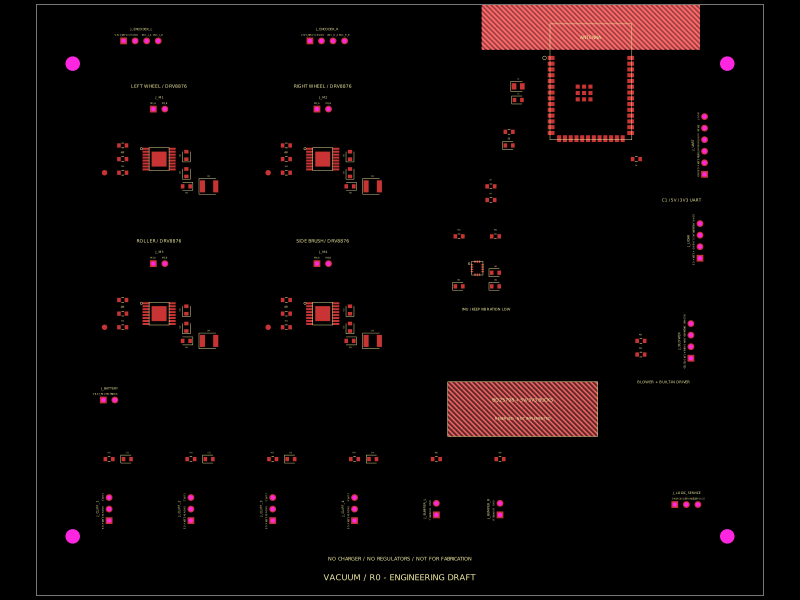 More from this authormohan-bee/tscircuit-robot-vacuum
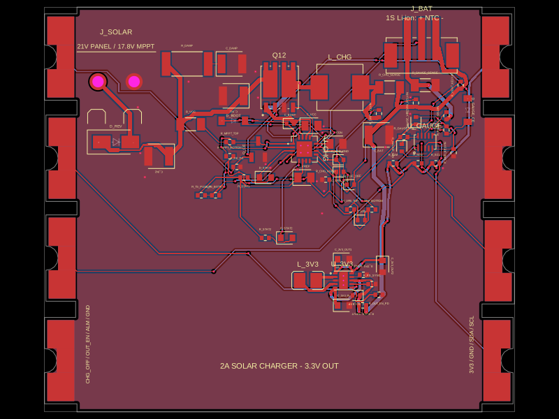 Similar packageShiboSoftwareDev/solar-battery-charger-moduleThis hardware setup integrates a solar panel, a lithium-ion battery, and a multi-rail buck converter with a battery charging IC, protection circuitry, and monitoring components, enabling solar power harvesting, battery charging, and power distribution in an embedded system.
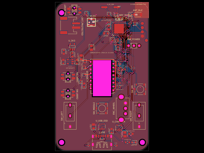 Discover something newMustafaMulla29/wireless-mouse-pcb