mohan-bee/compact-pir
Compact 3.3 V ESP8684 wireless motion/GPIO breakout board with LiPo regulation, 40 MHz crystal, U.FL antenna matching, digital PIR sensor, switched LED, decoupling, and dual 10-pin headers.
- Version
- 1.0.2
- License
- unset
- Stars
- 0
index.circuit.tsx
PCB
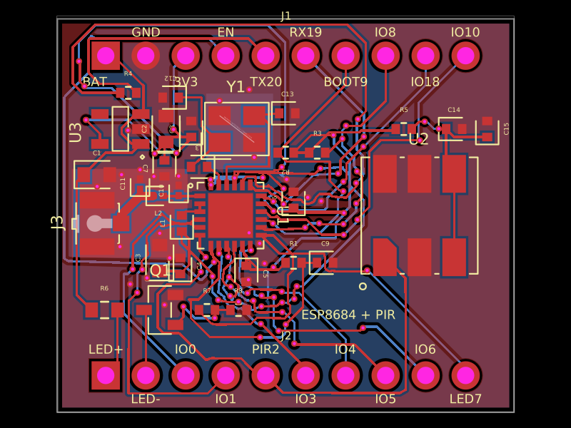
Schematic

import { Fragment } from "react"
import { partNumbers } from "./part-numbers"
import { ESP8684H4X } from "./imports/ESP8684H4X"
import { S18_L262B_2 } from "./imports/S18_L262B_2"
import { AP2112K_3_3TRG1 } from "./imports/AP2112K_3_3TRG1"
import { MMBT3904_RANGE_100_300_ } from "./imports/MMBT3904_RANGE_100_300_"
import { U_FL_R_SMT_1_80_ } from "./imports/U_FL_R_SMT_1_80_"
import { A_3225_40M_12PF_10PPM } from "./imports/A_3225_40M_12PF_10PPM"

const upperPins = ["BAT", "GND", "3V3", "EN", "TX20", "RX19", "BOOT9", "IO8", "IO18", "IO10"]
const lowerPins = ["LED+", "LED-", "IO0", "IO1", "PIR2", "IO3", "IO4", "IO5", "IO6", "LED7"]
const upperNets = ["VBAT", "GND", "V3V3", "EN", "UART_TX", "GPIO19", "GPIO9", "GPIO8", "GPIO18", "GPIO10"]
const lowerNets = ["LED_POS", "LED_NEG", "GPIO0", "GPIO1", "GPIO2", "GPIO3", "GPIO4", "GPIO5", "GPIO6", "GPIO7"]

export default function CompactMotionBoard() {
  return (
    <board width="29mm" height="25mm" layers={2} thickness="1mm" isViaInPadAllowed
      minTraceWidth="0.15mm" defaultTraceWidth="0.15mm" minViaHoleDiameter="0.2mm" minViaPadDiameter="0.4mm"
      minTraceToPadEdgeClearance="0.1mm" minViaEdgeToPadEdgeClearance="0.1mm"
      minViaHoleEdgeToViaHoleEdgeClearance="0.1mm" minPlatedHoleDrillEdgeToDrillEdgeClearance="0.1mm"
      minBoardEdgeClearance="0.3mm"
      pcbStyle={{ viaPadDiameter: "0.4mm", viaHoleDiameter: "0.2mm" }}
      title="ESP8684 motion / GPIO breakout — Pipeline9 development"
      autorouter="auto-local" autorouterVersion="beta_pipeline9" autorouterEffortLevel="2x" routeRemaining

      schAutoLayoutEnabled schTraceAutoLabelEnabled
      solderMaskColor="green">
      <net name="CHIP_TX" />
      <net name="EN" />
      <net name="GPIO0" />
      <net name="GPIO1" />
      <net name="GPIO10" />
      <net name="GPIO18" />
      <net name="GPIO19" />
      <net name="GPIO2" />
      <net name="GPIO3" />
      <net name="GPIO4" />
      <net name="GPIO5" />
      <net name="GPIO6" />
      <net name="GPIO7" />
      <net name="GPIO8" />
      <net name="GPIO9" />
      <net name="LED_BASE" />
      <net name="LED_NEG" />
      <net name="LED_POS" />
      <net name="RF_ANT" />
      <net name="RF_CHIP" />
      <net name="UART_TX" />
      <net name="XTAL_LOAD" />
      <net name="XTAL_N" />
      <net name="XTAL_P" />
      <net name="GND" isGroundNet />
      <net name="VBAT" isPowerNet nominalTraceWidth="0.15mm" />
      <net name="V3V3" isPowerNet nominalTraceWidth="0.15mm" />
      <net name="V3V3_RF" isPowerNet nominalTraceWidth="0.15mm" />
      <net name="PIR_VDD" isPowerNet />
      <schematicsection name="power" displayName="1S LiPo → 3.3 V / 600 mA" />
      <schematicsection name="mcu" displayName="ESP8684H4X / all 14 GPIOs exposed" />
      <schematicsection name="clock" displayName="40 MHz crystal — configure firmware" />
      <schematicsection name="rf" displayName="2.4 GHz / external 50 ohm antenna" />
      <schematicsection name="pir" displayName="Digital PIR / separate SB-F-11 lens" />
      <schematicsection name="led" displayName="Indicator LED / switched cathode" />
      <schematicsection name="headers" displayName="2 × 1x10 male headers / 2.54 mm" />

      <pinheader name="J1" {...partNumbers.J1} pinCount={10} pitch="2.54mm" gender="male"
        holeDiameter="1.1mm" platedDiameter="1.8mm" pcbX={0} pcbY={10.16}
        pinLabels={upperPins} schSectionName="headers" schWidth={0.675}
        connections={Object.fromEntries(upperNets.map((net, i) => [`pin${i + 1}`, `net.${net}`]))} />
      <pinheader name="J2" {...partNumbers.J2} pinCount={10} pitch="2.54mm" gender="male"
        holeDiameter="1.1mm" platedDiameter="1.8mm" pcbX={0} pcbY={-10.16}
        pinLabels={lowerPins.map(label => label.replace("+", "_POS").replace("-", "_NEG"))} schSectionName="headers" schWidth={0.865}
        connections={Object.fromEntries(lowerNets.map((net, i) => [`pin${i + 1}`, `net.${net}`]))} />
      {upperPins.map((text, i) => <Fragment key={`upper${i}`}><silkscreentext text={text}
        pcbX={i === 0 ? -12.1 : -11.43 + i * 2.54} pcbY={i % 2 === 0 ? 8.5 : 11.65} fontSize="0.8mm" /></Fragment>)}
      {lowerPins.map((text, i) => <Fragment key={`lower${i}`}><silkscreentext text={text}
        pcbX={-11.43 + i * 2.54} pcbY={i % 2 === 0 ? -8.5 : -11.65} fontSize="0.8mm" /></Fragment>)}

      <AP2112K_3_3TRG1 name="U3" {...partNumbers.U3} pcbX={-10.5} pcbY={5.5} pcbRotation={90} schSectionName="power" schWidth={1.865}
        connections={{ VIN: "net.VBAT", EN: "net.VBAT", GND: "net.GND", VOUT: "net.V3V3" }} />
      <capacitor name="C1" {...partNumbers.C1} capacitance="10uF" maxVoltageRating="10V" footprint="0603"
        pcbX={-12} pcbY={2.6} schRotation={-90} schSectionName="power"
        connections={{ pin1: "net.VBAT", pin2: "net.GND" }} />
      <capacitor name="C2" {...partNumbers.C2} capacitance="10uF" maxVoltageRating="10V" footprint="0603"
        pcbX={-7.6} pcbY={5.5} pcbRotation={90} schRotation={-90} schSectionName="power"
        connections={{ pin1: "net.V3V3", pin2: "net.GND" }} />

      <ESP8684H4X name="U1" {...partNumbers.U1} pcbX={-3.5} pcbY={0} pcbRotation={270} schSectionName="mcu" schWidth={2.72} schHeight={3} schMarginX="2mm"
        schPinArrangement={{ leftSide: [2,3,11,17,21,24,7,22,23,1,25], rightSide: [4,5,6,8,9,10,12,13,14,15,16,18,19,20] }}
        connections={{
          pin1: "net.RF_CHIP", pin2: "net.V3V3_RF", pin3: "net.V3V3_RF",
          pin4: "net.GPIO0", pin5: "net.GPIO1", pin6: "net.GPIO2", pin7: "net.EN",
          pin8: "net.GPIO3", pin9: "net.GPIO4", pin10: "net.GPIO5", pin11: "net.V3V3",
          pin12: "net.GPIO6", pin13: "net.GPIO7", pin14: "net.GPIO8", pin15: "net.GPIO9",
          pin16: "net.GPIO10", pin17: "net.V3V3", pin18: "net.GPIO18", pin19: "net.GPIO19",
          pin20: "net.CHIP_TX", pin21: "net.V3V3", pin22: "net.XTAL_N",
          pin23: "net.XTAL_P", pin24: "net.V3V3", pin25: "net.GND",
        }} />
      <inductor name="L1" {...partNumbers.L1} inductance="2nH" maxCurrentRating="600mA" footprint="0402"
        pcbX={-6.6} pcbY={-0.5} pcbRotation={90} schSectionName="power"
        connections={{ pin1: "net.V3V3", pin2: "net.V3V3_RF" }} />
      {[
        { name: "C3", value: "10uF", fp: "0603", x: -8, y: -2.7, net: "V3V3" },
        { name: "C4", value: "100nF", fp: "0402", x: -6.7, y: -3.2, net: "V3V3" },
        { name: "C5", value: "100nF", fp: "0402", x: -2.5, y: -3.7, net: "V3V3" },
        { name: "C6", value: "100nF", fp: "0402", x: 0.5, y: 1.0, net: "V3V3" },
        { name: "C7", value: "1uF", fp: "0402", x: -7.7, y: 3, net: "V3V3" },
        { name: "C8", value: "10nF", fp: "0402", x: -6, y: 5.5, net: "V3V3" },
      ].map(c => <capacitor key={c.name} name={c.name} {...partNumbers[c.name]} capacitance={c.value} maxVoltageRating="10V"
        footprint={c.fp} pcbX={c.x} pcbY={c.y} pcbRotation={c.name === "C5" || c.name === "C7" ? 270 : 90} schRotation={-90} schSectionName="power"
        connections={{ pin1: `net.${c.net}`, pin2: "net.GND" }} />)}
      <resistor name="R1" {...partNumbers.R1} resistance="10k" footprint="0402" pcbX={0.5} pcbY={-3} schRotation={-90} schSectionName="mcu" connections={{ pin1: "net.V3V3", pin2: "net.EN" }} />
      <capacitor name="C9" {...partNumbers.C9} capacitance="1uF" maxVoltageRating="10V" footprint="0402"
        pcbX={2.5} pcbY={-3} schRotation={-90} schSectionName="mcu" connections={{ pin1: "net.EN", pin2: "net.GND" }} />
      <resistor name="R2" {...partNumbers.R2} resistance="10k" footprint="0402" pcbX={0} pcbY={4} pcbRotation={180} schRotation={-90} schSectionName="mcu" connections={{ pin1: "net.V3V3", pin2: "net.GPIO9" }} />
      <resistor name="R3" {...partNumbers.R3} resistance="10k" footprint="0402" pcbX={2} pcbY={4} schRotation={-90} schSectionName="mcu" connections={{ pin1: "net.V3V3", pin2: "net.GPIO8" }} />
      <resistor name="R4" {...partNumbers.R4} resistance="499" footprint="0402" pcbX={-10} pcbY={7.8} schSectionName="mcu" connections={{ pin1: "net.CHIP_TX", pin2: "net.UART_TX" }} />

      {/* Initial RF tuning values; finalize the 50 ohm feed against the fabrication stackup. */}
      <U_FL_R_SMT_1_80_ name="J3" {...partNumbers.J3} pcbX={-11.5} pcbY={-0.5} pcbRotation={90} schSectionName="rf" schWidth={1.96}
        connections={{ SIG: "net.RF_ANT", GND1: "net.GND", GND2: "net.GND" }} />
      <capacitor name="C10" {...partNumbers.C10} capacitance="1.5pF" maxVoltageRating="25V" footprint="0201"
        pcbX={-6.8} pcbY={1.6} pcbRotation={90} schRotation={-90} schSectionName="rf"
        connections={{ pin1: "net.RF_CHIP", pin2: "net.GND" }} />
      <inductor name="L2" {...partNumbers.L2} inductance="2.7nH" footprint="0201" schMarginX="0.5mm" schMarginY="0.5mm"
        pcbX={-8.1} pcbY={1.25} schSectionName="rf"
        connections={{ pin1: "net.RF_ANT", pin2: "net.RF_CHIP" }} />
      <capacitor name="C11" {...partNumbers.C11} capacitance="1.5pF" maxVoltageRating="25V" footprint="0201"
        pcbX={-9.25} pcbY={2} pcbRotation={90} schRotation={-90} schSectionName="rf"
        connections={{ pin1: "net.RF_ANT", pin2: "net.GND" }} />

      <A_3225_40M_12PF_10PPM name="Y1" {...partNumbers.Y1} loadCapacitance="12pF" pcbX={-3.1} pcbY={5.5} schSectionName="clock"
        connections={{ pin1: "net.XTAL_LOAD", pin2: "net.GND", pin3: "net.XTAL_N", pin4: "net.GND" }} />
      <inductor name="L3" {...partNumbers.L3} inductance="24nH" footprint="0402" pcbX={-5.5} pcbY={3.1} pcbRotation={180} schSectionName="clock" connections={{ pin1: "net.XTAL_P", pin2: "net.XTAL_LOAD" }} />
      <capacitor name="C12" {...partNumbers.C12} capacitance="18pF" maxVoltageRating="25V" footprint="0402"
        pcbX={-7.3} pcbY={7.5} pcbRotation={180} schRotation={-90} schSectionName="clock"
        connections={{ pin1: "net.XTAL_LOAD", pin2: "net.GND" }} />
      <capacitor name="C13" {...partNumbers.C13} capacitance="18pF" maxVoltageRating="25V" footprint="0402"
        pcbX={0.1} pcbY={6.5} schRotation={-90} schSectionName="clock"
        connections={{ pin1: "net.XTAL_N", pin2: "net.GND" }} />

      <S18_L262B_2 name="U2" {...partNumbers.U2} pcbX={8.5} pcbY={0} schSectionName="pir" schWidth={2.15} schHeight={0.8}
        connections={{ REL: "net.GPIO2", ONTIME: "net.GND", OEN: "net.PIR_VDD",
          VDD: "net.PIR_VDD", SENS: "net.GND", VSS: "net.GND" }} />
      <resistor name="R5" {...partNumbers.R5} resistance="100" footprint="0402" pcbX={7.5} pcbY={5.5} schRotation={-90} schSectionName="pir" connections={{ pin1: "net.V3V3", pin2: "net.PIR_VDD" }} />
      <capacitor name="C14" {...partNumbers.C14} capacitance="1uF" maxVoltageRating="10V" footprint="0402"
        pcbX={10.7} pcbY={5.5} schRotation={-90} schSectionName="pir" connections={{ pin1: "net.PIR_VDD", pin2: "net.GND" }} />
      <capacitor name="C15" {...partNumbers.C15} capacitance="100nF" maxVoltageRating="10V" footprint="0402"
        pcbX={12.8} pcbY={5.5} pcbRotation={90} schRotation={-90} schSectionName="pir" connections={{ pin1: "net.PIR_VDD", pin2: "net.GND" }} />

      <MMBT3904_RANGE_100_300_ name="Q1" {...partNumbers.Q1} pcbX={-8} pcbY={-6} schSectionName="led" connections={{ B: "net.LED_BASE", E: "net.GND", C: "net.LED_NEG" }} />
      <resistor name="R6" {...partNumbers.R6} resistance="150" footprint="0603" pcbX={-11.5} pcbY={-6} schRotation={-90} schSectionName="led" connections={{ pin1: "net.VBAT", pin2: "net.LED_POS" }} />
      <resistor name="R7" {...partNumbers.R7} resistance="2.2k" footprint="0402" pcbX={-5} pcbY={-6} schSectionName="led" connections={{ pin1: "net.GPIO7", pin2: "net.LED_BASE" }} />
      <resistor name="R8" {...partNumbers.R8} resistance="100k" footprint="0402" pcbX={-3} pcbY={-6} schRotation={-90} schSectionName="led" connections={{ pin1: "net.LED_BASE", pin2: "net.GND" }} />

      <trace name="RF_CHIP_FEED" from=".U1 > .pin1" to=".L2 > .pin2" thickness="0.18mm"
        pcbPath={[".U1 > .pin1", { x: -1.25, y: -3.3 }, ".L2 > .pin2"]} />
      <trace name="RF_CHIP_SHUNT" from=".C10 > .pin1" to=".L2 > .pin2" thickness="0.18mm"
        pcbPath={[".C10 > .pin1", { x: -0.35, y: -0.0 }, ".L2 > .pin2"]} />
      <trace name="RF_ANT_FEED" from=".L2 > .pin1" to=".J3 > .pin1" thickness="0.55mm"
        pcbPath={[".L2 > .pin1", { x: -1.15, y: 0.0 }, { x: -2.35, y: -1.2 }, ".J3 > .pin1"]} />
      <trace name="RF_ANT_SHUNT" from=".C11 > .pin1" to=".L2 > .pin1" thickness="0.18mm"
        pcbPath={[".C11 > .pin1", { x: -0.75, y: -0.0 }, ".L2 > .pin1"]} />
      <trace name="XTAL_P_FEED" from=".U1 > .pin23" to=".L3 > .pin1" thickness="0.15mm"
        pcbPath={[".U1 > .pin23", { x: -2.6, y: -0.75 }, ".L3 > .pin1"]} />
      <trace name="XTAL_LOAD_FEED" from=".L3 > .pin2" to=".Y1 > .pin1" thickness="0.15mm"
        pcbPath={[".L3 > .pin2", ".Y1 > .pin1"]} />
      <trace name="XTAL_N_FEED" from=".U1 > .pin22" to=".Y1 > .pin3" thickness="0.15mm"
        pcbPath={[".U1 > .pin22", { x: -3.1, y: -0.25 }, { x: -3.1, y: 2.45 },
          { x: -5.8, y: 2.45 }, { x: -6.35, y: 1.9 }, ".Y1 > .pin3"]} />

      <trace name="XTAL_LOAD_CAP" from=".C12 > .pin1" to=".Y1 > .pin1" thickness="0.15mm"
        pcbPath={[".C12 > .pin1", {x:-1.95,y:0}, {x:-1.95,y:1.8}, ".Y1 > .pin1"]} />
      <trace name="XTAL_N_CAP" from=".C13 > .pin1" to=".Y1 > .pin3" thickness="0.15mm" pcbPath={[".C13 > .pin1", ".Y1 > .pin3"]} />
      <copperpour name="top_ground" layer="top" connectsTo="net.GND" clearance="0.15mm" boardEdgeMargin="0.3mm" />
      <copperpour name="ground_plane" layer="bottom" connectsTo="net.GND" clearance="0.2mm" boardEdgeMargin="0.3mm" />
      <copperpour name="rf_reference" layer="bottom" connectsTo="net.GND" unbroken clearance="0.15mm"
        outline={[{x:-13.7,y:-2.8},{x:-6.1,y:-2.8},{x:-6.1,y:3.1},{x:-13.7,y:3.1}]} />
      <copperpour name="rf_coplanar_ground" layer="top" connectsTo="net.GND" clearance="0.12mm"
        outline={[{x:-13.7,y:-2.8},{x:-6.1,y:-2.8},{x:-6.1,y:3.1},{x:-13.7,y:3.1}]} />
      <copperpour name="clock_reference" layer="bottom" connectsTo="net.GND" unbroken clearance="0.15mm"
        outline={[{x:-5.2,y:2.8},{x:-0.65,y:2.8},{x:-0.65,y:7.9},{x:-5.2,y:7.9}]} />
      <silkscreentext text="ESP8684 + PIR" pcbX={4} pcbY={-6.3} fontSize="0.8mm" />
    </board>
  )
}
Related Packages
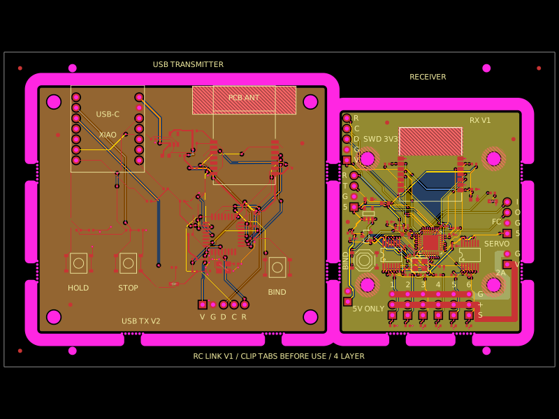 More from this authormohan-bee/rc-link-breakaway-panelA four-layer RC link panel combining an STM32/E28 2.4‑GHz transmitter with USB-RP2040 socket and an STM32/E28 receiver providing six buffered PWM servo outputs, regulated 3.3‑V power, headers, controls, and protection/decoupling.
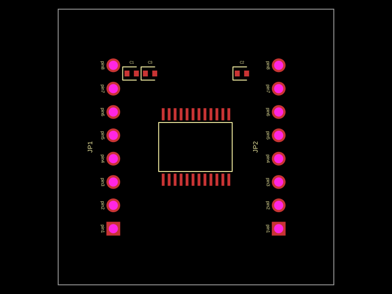 Similar packageimrishabh18/motor-driver-breakout"A 30x30mm TB6612FNG motor driver board with dual 8-pin headers and bypass capacitors for motor control and power regulation"
This summary captures the key physical characteristics:
- Uses TB6612FNG motor driver chip
- 30x30mm board size
- Dual 8-pin headers (JP1 and JP2)
- Includes decoupling capacitors (C1, C2, C3)
- Purpose is motor control and power management
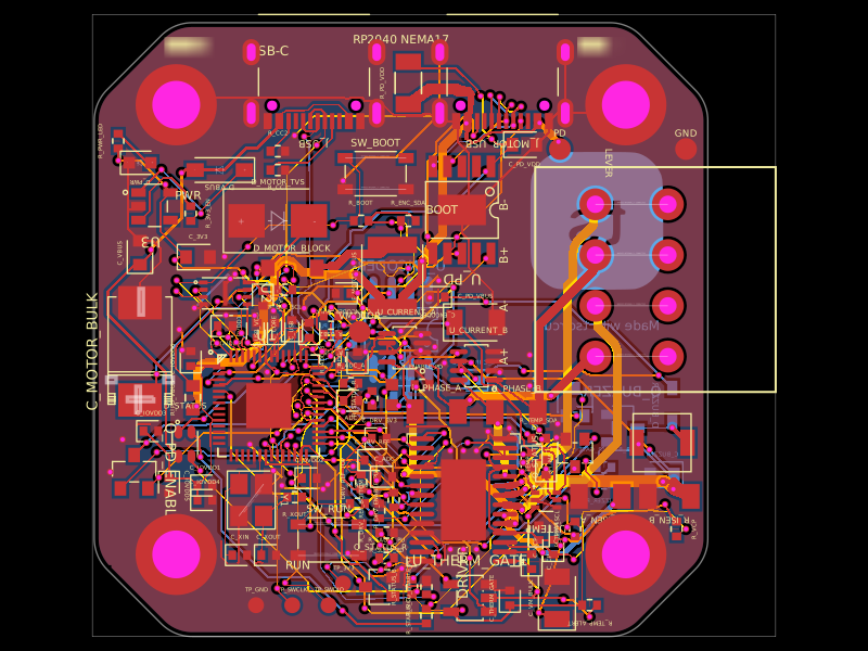 Discover something newastra/nema17-stepper-motor-controller-spring-clamp-rp2040A 4-layer RP2040 controller board that negotiates USB‑C PD motor power and drives a NEMA17 stepper via a DRV8825, with current sensing, thermal shutdown, RGB status LED, buzzer alarm, optional AS5600 encoder, protection/filtering, and test points.