laydas/grow_cabinet_controller
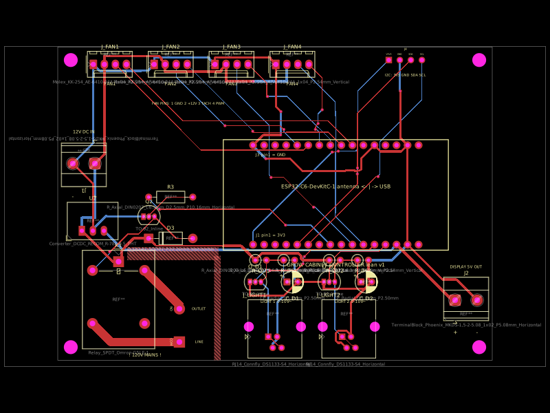
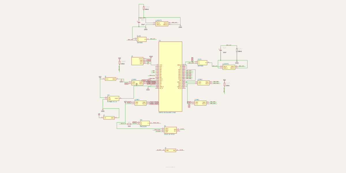
An ESP32-C6-based grow-cabinet controller board with four PWM/tach fan outputs, two filtered 0–10 V light-dimmer outputs, a 12 V master relay, protected dual 5 V supplies, USB power, and I²C/GPIO headers.
- Version
- 0.0.1
- License
- unset
- Stars
- 0
index.tsx
PCB
Schematic
/**
 * Grow Cabinet Controller (lean) — ESP32-C6-DevKitC-1
 *
 * Only the parts that do the job.  All through-hole.  Single 12V DC input.
 *
 *  - 4x PC fan headers.  PWM driven straight from 3.3V GPIO, tach read with the ESP's internal pull-up.
 *  - 2x 0-10V dimmer outputs (RJ11 jacks) for the ViparSpectra P1000 dimming ports:
 *      2N7000 chops 12V, 10k pull-up + 68k to ground caps the output at ~10.5V, 10uF smooths it.
 *  - 1x master relay (G5LE-14 DC12) switching the outlet hot: NPN driver, base resistor, flyback diode.
 *  - 12V in on a screw terminal -> one Recom R-78B5.0-1.5 -> 5V to the DevKit and to a 5V terminal
 *    for the display.
 *  - 1x I2C header (3V3 GND SDA SCL) for the SHT31 breakout (breakout carries its own pull-ups).
 *
 * GPIO map:
 *   FAN1..4 PWM  = IO18 IO19 IO20 IO21   (direct drive, NOT inverted)
 *   FAN1..4 TACH = IO22 IO23 IO10 IO11   (internal pull-up)
 *   DIM1 DIM2    = IO2  IO3              (inverted: 100% duty = 0V = light off)
 *   RELAY        = IO1                   (high = relay on)
 *   I2C SDA/SCL  = IO6 / IO7
 */

import { Fragment } from "react"

const FP = {
  to92: "kicad:Package_TO_SOT_THT/TO-92_Inline",
  resV: "kicad:Resistor_THT/R_Axial_DIN0207_L6.3mm_D2.5mm_P2.54mm_Vertical",
  res: "kicad:Resistor_THT/R_Axial_DIN0207_L6.3mm_D2.5mm_P10.16mm_Horizontal",
  capElec: "kicad:Capacitor_THT/CP_Radial_D5.0mm_P2.50mm",
  do41: "kicad:Diode_THT/D_DO-41_SOD81_P10.16mm_Horizontal",
  relay: "kicad:Relay_THT/Relay_SPDT_Omron-G5LE-1",
  rj11: "kicad:Connector_RJ/RJ14_Connfly_DS1133-S4_Horizontal",
  fanHeader: "kicad:Connector_Molex/Molex_KK-254_AE-6410-04A_1x04_P2.54mm_Vertical",
  recom: "kicad:Converter_DCDC/Converter_DCDC_RECOM_R-78E-0.5_THT",
  term508: "kicad:TerminalBlock_Phoenix/TerminalBlock_Phoenix_MKDS-1,5-2-5.08_1x02_P5.08mm_Horizontal",
  term762: "pinrow2_p7.62mm_id1.3mm_od2.6mm",
  hdr4: "pinrow4",
}

// KiCad footprints are anchored on pad 1.  at() takes a desired CENTRE and returns the anchor.
const CENTER_OFFSET: Record<string, [number, number]> = {
  to92: [1.27, 0], resV: [1.27, 0], res: [5.08, 0], capElec: [1.25, 0], do41: [5.08, 0],
  relay: [0, -8.65], rj11: [1.55, 1.8], fanHeader: [3.81, 0], recom: [2.45, 2.25],
  term508: [2.55, 0.2], term762: [0, 0], hdr4: [0, 0],
}
const at = (fp: keyof typeof FP, cx: number, cy: number, rot = 0) => {
  const [dx, dy] = CENTER_OFFSET[fp]
  const r = (rot * Math.PI) / 180
  const ox = dx * Math.cos(r) - dy * Math.sin(r)
  const oy = dx * Math.sin(r) + dy * Math.cos(r)
  return { footprint: FP[fp], pcbX: +(cx - ox).toFixed(3), pcbY: +(cy - oy).toFixed(3), pcbRotation: rot }
}

// KiCad diode footprints: pad 1 = cathode (band), pad 2 = anode
const K = "pin1"
const A = "pin2"

// ---------- DevKitC-1 socket footprint (antenna LEFT, USB-C RIGHT) ----------
const ROW_Y = 22.86 / 2
const PIN1_X = -19.05
const J1_PINS = ["3V3", "RST", "IO4", "IO5", "IO6", "IO7", "IO0", "IO1", "IO8", "IO10", "IO11", "IO2", "IO3", "5V", "GND_A", "NC_A"]
const J3_PINS = ["GND_B", "TX", "RX", "IO15", "IO23", "IO22", "IO21", "IO20", "IO19", "IO18", "IO9", "GND_C", "IO13", "IO12", "GND_D", "NC_B"]
const devkitPinLabels: Record<string, string> = {}
J1_PINS.forEach((n, i) => (devkitPinLabels[`pin${i + 1}`] = n))
J3_PINS.forEach((n, i) => (devkitPinLabels[`pin${i + 17}`] = n))

const DevKitFootprint = () => (
  <footprint>
    {J1_PINS.map((n, i) => (
      // @ts-expect-error key
      <platedhole key={`j1-${i}`} shape="circle" holeDiameter="1.0mm" outerDiameter="1.8mm"
        pcbX={PIN1_X + i * 2.54} pcbY={-ROW_Y} portHints={[`pin${i + 1}`]} />
    ))}
    {J3_PINS.map((n, i) => (
      // @ts-expect-error key
      <platedhole key={`j3-${i}`} shape="circle" holeDiameter="1.0mm" outerDiameter="1.8mm"
        pcbX={PIN1_X + i * 2.54} pcbY={ROW_Y} portHints={[`pin${i + 17}`]} />
    ))}
    <silkscreenrect pcbX={0} pcbY={0} width="51.8mm" height="25.4mm" strokeWidth="0.2mm" filled={false} />
    <silkscreentext text="ESP32-C6-DevKitC-1   antenna <- | -> USB" pcbX={0} pcbY={2} fontSize={1.2} />
    <silkscreentext text="J1 pin1 = 3V3" pcbX={PIN1_X + 4} pcbY={-ROW_Y + 2.2} fontSize={0.9} />
    <silkscreentext text="J3 pin1 = GND" pcbX={PIN1_X + 4} pcbY={ROW_Y - 2.2} fontSize={0.9} />
  </footprint>
)

// ---------- layout (component centres, mm from board centre) ----------
const DEVKIT_POS = { x: 14, y: 2 }        // outline x -11.9..39.9, y -10.7..14.7
const FAN_X = [-38, -24, -10, 4]
const DIM_X = [0, 17]

export default () => (
  <board width="100mm" height="72mm" defaultTraceWidth="0.25mm" minTraceWidth="0.2mm"
    minViaHoleDiameter="0.3mm" minViaPadDiameter="0.7mm">
    <net name="V12" isPowerNet nominalTraceWidth="0.6mm" />
    <net name="V5" isPowerNet nominalTraceWidth="0.6mm" />
    <net name="GND" isGroundNet nominalTraceWidth="0.5mm" />
    <net name="AC_COM" nominalTraceWidth="2mm" />
    <net name="AC_NO" nominalTraceWidth="2mm" />

    <hole name="H1" diameter="3.2mm" pcbX={-47} pcbY={33} />
    <hole name="H2" diameter="3.2mm" pcbX={47} pcbY={33} />
    <hole name="H3" diameter="3.2mm" pcbX={-47} pcbY={-33} />
    <hole name="H4" diameter="3.2mm" pcbX={47} pcbY={-33} />

    {/* ---------- DevKit ---------- */}
    <chip name="U1" footprint={<DevKitFootprint />} pinLabels={devkitPinLabels}
      pcbX={DEVKIT_POS.x} pcbY={DEVKIT_POS.y}
      manufacturerPartNumber="ESP32-C6-DevKitC-1-N8"
      schWidth={3} schHeight={9}
      schPinArrangement={{
        leftSide: { direction: "top-to-bottom", pins: J1_PINS },
        rightSide: { direction: "top-to-bottom", pins: J3_PINS },
      }}
      connections={{
        "5V": "net.V5",
        GND_A: "net.GND", GND_B: "net.GND", GND_C: "net.GND", GND_D: "net.GND",
        "3V3": "net.V3V3",
        IO6: "net.SDA", IO7: "net.SCL",
        IO1: "net.RELAY_CTL",
        IO2: "net.DIM1_PWM", IO3: "net.DIM2_PWM",
        IO18: "net.FAN1_PWM", IO19: "net.FAN2_PWM", IO20: "net.FAN3_PWM", IO21: "net.FAN4_PWM",
        IO22: "net.FAN1_TACH", IO23: "net.FAN2_TACH", IO10: "net.FAN3_TACH", IO11: "net.FAN4_TACH",
      }} />

    {/* ---------- power: 12V in -> Recom -> 5V ---------- */}
    <chip name="J1" {...at("term508", -44, 9, 180)} pinLabels={{ pin1: "V12", pin2: "GND" }}
      connections={{ V12: "net.V12", GND: "net.GND" }} />
    <silkscreentext text="12V DC IN" pcbX={-44} pcbY={16.5} fontSize={1} />
    <silkscreentext text="+" pcbX={-41.5} pcbY={1.7} fontSize={1.2} />
    <silkscreentext text="-" pcbX={-46.5} pcbY={1.7} fontSize={1.2} />
    <chip name="U2" {...at("recom", -42, -4, 0)} pinLabels={{ pin1: "VIN", pin2: "GND", pin3: "VOUT" }}
      manufacturerPartNumber="R-78B5.0-1.5"
      connections={{ VIN: "net.V12", GND: "net.GND", VOUT: "net.V5" }} />
    <chip name="J2" {...at("term508", 44, -22, 0)} pinLabels={{ pin1: "V5", pin2: "GND" }}
      connections={{ V5: "net.V5", GND: "net.GND" }} />
    <silkscreentext text="DISPLAY 5V OUT" pcbX={44} pcbY={-14.5} fontSize={0.9} />
    <silkscreentext text="+" pcbX={41.5} pcbY={-29.5} fontSize={1.2} />
    <silkscreentext text="-" pcbX={46.5} pcbY={-29.5} fontSize={1.2} />

    {/* ---------- fans: header only.  1 GND  2 +12V  3 TACH  4 PWM ---------- */}
    {FAN_X.map((x, i) => {
      const n = i + 1
      return (
        <Fragment key={`fan-${n}`}>
          <chip name={`J_FAN${n}`} {...at("fanHeader", x, 32, 0)}
            pinLabels={{ pin1: "GND", pin2: "V12", pin3: "TACH", pin4: "PWM" }}
            connections={{ GND: "net.GND", V12: "net.V12", TACH: `net.FAN${n}_TACH`, PWM: `net.FAN${n}_PWM` }} />
          <silkscreentext text={`FAN${n}`} pcbX={x} pcbY={27.5} fontSize={1} />
        </Fragment>
      )
    })}
    <silkscreentext text="FAN PINS: 1 GND  2 +12V  3 TACH  4 PWM" pcbX={-20} pcbY={23} fontSize={0.8} />

    {/* ---------- I2C header ---------- */}
    <pinheader name="J4" pinCount={4} pitch="2.54mm" gender="male" {...at("hdr4", 30, 33, 0)}
      pinLabels={["V3V3", "GND", "SDA", "SCL"]}
      connections={{ V3V3: "net.V3V3", GND: "net.GND", SDA: "net.SDA", SCL: "net.SCL" }} />
    <silkscreentext text="I2C: 3V3 GND SDA SCL" pcbX={30} pcbY={29.5} fontSize={0.8} />

    {/* ---------- dimmers: 2N7000 chops 12V; 10k up, 68k down, 10uF ---------- */}
    {DIM_X.map((x, i) => {
      const n = i + 1
      return (
        <Fragment key={`light-${n}`}>
          <chip name={`J_LIGHT${n}`} {...at("rj11", x, -28.8, 0)}
            pinLabels={{ pin1: "DIM_A", pin2: "GND_A", pin3: "GND_B", pin4: "DIM_B" }}
            connections={{ DIM_A: `net.DIM${n}_OUT`, DIM_B: `net.DIM${n}_OUT`, GND_A: "net.GND", GND_B: "net.GND" }} />
          <silkscreentext text={`LIGHT ${n}  0-10V`} pcbX={x} pcbY={-22.5} fontSize={0.9} />
          {/* 2N7000 TO-92: 1 = S, 2 = G, 3 = D */}
          <chip name={`Q_D${n}`} {...at("to92", x - 4.5, -18, 0)} pinLabels={{ pin1: "S", pin2: "G", pin3: "D" }}
            manufacturerPartNumber="2N7000"
            connections={{ S: "net.GND", G: `net.DIM${n}_PWM`, D: `net.DIM${n}_OUT` }} />
          <capacitor name={`C_D${n}`} capacitance="10uF" polarized {...at("capElec", x + 4, -18, 0)}
            connections={{ pin1: `net.DIM${n}_OUT`, pin2: "net.GND" }} />
          <resistor name={`R_DU${n}`} resistance="10k" {...at("resV", x - 3.25, -13, 0)}
            connections={{ pin1: "net.V12", pin2: `net.DIM${n}_OUT` }} />
          <resistor name={`R_DL${n}`} resistance="68k" {...at("resV", x + 3.25, -13, 0)}
            connections={{ pin1: `net.DIM${n}_OUT`, pin2: "net.GND" }} />
        </Fragment>
      )
    })}

    {/* ---------- master relay.  G5LE pads: 1,2 coil ; 3 COM ; 4 NC ; 5 NO ---------- */}
    <chip name="K1" {...at("relay", -36, -22, 0)}
      pinLabels={{ pin1: "COIL1", pin2: "COIL2", pin3: "COM", pin4: "NC", pin5: "NO" }}
      manufacturerPartNumber="G5LE-14 DC12"
      connections={{ COIL1: "net.V12", COIL2: "net.RELAY_COIL", COM: "net.AC_COM", NO: "net.AC_NO" }} />
    <chip name="J3" {...at("term762", -22, -28, 90)} pinLabels={{ pin1: "COM", pin2: "NO" }}
      connections={{ COM: "net.AC_COM", NO: "net.AC_NO" }} />
    <silkscreentext text="LINE" pcbX={-17.5} pcbY={-31.8} fontSize={0.8} />
    <silkscreentext text="OUTLET" pcbX={-17.5} pcbY={-24.2} fontSize={0.8} />
    <silkscreentext text="! 120V MAINS !" pcbX={-30} pcbY={-34.8} fontSize={1} />
    {/* routing fence: keeps low-voltage traces out of the mains corner */}
    <keepout shape="rect" pcbX={-13.25} pcbY={-24} width="1.5mm" height="24mm" />
    <keepout shape="rect" pcbX={-23.5} pcbY={-11.5} width="21mm" height="3mm" excludeRefs={[".K1"]} />
    {/* PN2222A TO-92: 1 = E, 2 = B, 3 = C */}
    <chip name="Q2" {...at("to92", -29, -3, 0)} pinLabels={{ pin1: "E", pin2: "B", pin3: "C" }}
      manufacturerPartNumber="PN2222A"
      connections={{ E: "net.GND", B: ".R3 > .pin2", C: "net.RELAY_COIL" }} />
    <resistor name="R3" resistance="1k" {...at("res", -24, 1.5, 0)}
      connections={{ pin1: "net.RELAY_CTL" }} />
    <diode name="D3" {...at("do41", -24, -8, 0)} manufacturerPartNumber="1N4007"
      connections={{ [A]: "net.RELAY_COIL", [K]: "net.V12" }} />

    <silkscreentext text="GROW CABINET CONTROLLER  lean v1" pcbX={14} pcbY={-14} fontSize={1.2} />
  </board>
)
Related Packages
 Similar packagegokul/usb3-sd-hubEngineering draft: four-layer, computer-powered USB 3 hub with one USB-C host socket, two USB-C and two USB-A accessory sockets, and a full-size SD slot. Board and three schematic previews are available. Routing and production checks are incomplete; not fabrication ready.
 Discover something newgokul/fieldkit-usbUSB-C-powered ESP32-S3 Wi-Fi/Bluetooth handheld with an SMD 128x32 OLED, six navigation buttons, USB-C power/data, complete checked routing, and four native schematic sheets.