imrishabh18/nema-23-stepper-controller
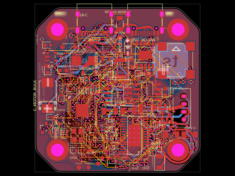
A 57 mm four-layer RP2040 NEMA23 stepper-controller PCB with USB‑C/USB‑PD power input, protected motor rail, DRV8452 dual-winding driver, bidirectional current sensing, temperature/enable interlock, optional magnetic encoder, RGB LED and buzzer status indicators, and motor/test connectors.
- Version
- 1.2.3
- License
- unset
- Stars
- 0
usb-pd-power.tsx
import { CH224Q } from "./imports/CH224Q";
import { TPS26630RGER } from "./imports/TPS26630RGER";
import { USB4105_GF_A } from "./imports/USB4105_GF_A";
import { TCA9517DGKR } from "./imports/TCA9517DGKR";
const pd = { schSheetName: "usb_pd", schSectionName: "usb_pd" };
const protection = { schSheetName: "power_settings", schSectionName: "power_protection" };
const efuseNets = { IN1: "VFUSED", IN2: "VFUSED", IN_SYS: "VFUSED", GND: "GND", EP: "GND",
    UVLO: "UVLO", OVP: "OVP", dVdT: "SLEW", ILIM: "ILIM", N_SHDN: "POWER_ARM",
    N_FLT: "POWER_FAULT_N", PGTH: "PGTH", PGOOD: "TEMP_OK", OUT1: "VSWITCHED", OUT2: "VSWITCHED" };
// CH224Q V2.1: 210 kohm requests 28 V. No e-marker emulation: use a real
// EPR-rated cable and a charger offering 28 V / 5 A on the selected port.
export function UsbPdPower() {
    return <>
  <schematicsheet sheetSize="A4" name="pd_control" displayName="Programmable USB-PD — buffered I2C" sheetIndex={10}>
    <schematicsection name="pd_control" displayName="I2C buffer — isolates the unpowered PD controller"/>
  </schematicsheet>
  <TCA9517DGKR name="U_PD_BUFFER" pcbX={-16} pcbY={24} pcbRotation={0} schSheetName="pd_control" schSectionName="pd_control" connections={{ VCCA: "net.V3V3", VCCB: "net.V3V3", GND: "net.GND", EN: "net.PD_BUS_ENABLE",
            SDAA: "net.I2C0_SDA", SCLA: "net.I2C0_SCL", SDAB: "net.PD_SDA", SCLB: "net.PD_SCL" }}/>
  {/* MCU-side pull-ups are R_ENC_SDA/SCL; CH224Q provides its own 7–15 kΩ pull-ups.
            Both buffer supplies are logic 3.3 V. Its B pins remain high-Z with logic off.
            Keep this branch disabled when the motor USB source is absent. */}
  <resistor schMarginX={0.35} schMarginY={0.7} name="R_PD_BUS_OFF" resistance="100k" footprint="0402" pcbX={-14} pcbY={19.95} schOrientation="vertical" schSheetName="pd_control" schSectionName="pd_control" connections={{ pin1: "net.PD_BUS_ENABLE", pin2: "net.GND" }}/>
  {[0, 1].map(i => <capacitor schMarginX={0.35} schMarginY={0.7} key={i} name={`C_PD_BUFFER_${i}`} capacitance="100nF" footprint="0402" pcbX={-18.8} pcbY={i ? 27.1 : 21.6} schOrientation="vertical" schSheetName="pd_control" schSectionName="pd_control" connections={{ pin1: "net.V3V3", pin2: "net.GND" }}/>)}
  <USB4105_GF_A name="J_USB_POWER" pcbX={9} pcbY={22.9} pcbRotation={180} {...pd} schSheetName="power" schSectionName="power" noConnect={["SBU1", "SBU2"]} connections={{ GND1: "net.GND", GND2: "net.GND", GND3: "net.GND", pin20: "net.GND",
            EH1: "net.GND", EH2: "net.GND", EH3: "net.GND", EH4: "net.GND",
            VBUS1: "net.VIN", VBUS2: "net.VIN", VBUS3: "net.VIN", VBUS4: "net.VIN",
            CC1: "net.PD_CC1", CC2: "net.PD_CC2", DP1: "net.PD_DP", DP2: "net.PD_DP", DN1: "net.PD_DM", DN2: "net.PD_DM" }}/>
  <CH224Q name="U_PD" pcbX={4.5} pcbY={16} {...pd} connections={{ VHV: "net.VIN", VBUS: "net.VIN", EP: "net.GND", CC1: "net.PD_CC1", CC2: "net.PD_CC2",
            DP: "net.PD_DP", DM: "net.PD_DM", CFG1: "net.PD_CFG", PG: "net.PD_PG_N", CFG2_SCL: "net.PD_SCL", CFG3_SDA: "net.PD_SDA" }}/>
  <capacitor schMarginX={0.35} schMarginY={0.7} name="C_PD" capacitance="1uF" maxVoltageRating="50V" footprint="0805" pcbX={1} pcbY={16} schOrientation="vertical" {...pd} connections={{ pin1: "net.VIN", pin2: "net.GND" }}/>
  <resistor schMarginX={0.35} schMarginY={0.7} name="R_PD_CFG" resistance="210k" footprint="0603" pcbX={4.5} pcbY={19} schOrientation="vertical" {...pd} connections={{ pin1: "net.PD_CFG", pin2: "net.GND" }}/>
  <resistor schMarginX={0.35} schMarginY={0.7} name="R_PD_PG" resistance="10k" footprint="0603" pcbX={1} pcbY={19} schOrientation="vertical" {...pd} connections={{ pin1: "net.V3V3", pin2: "net.PD_PG_N" }}/>
  <fuse schMarginX={1.1} schMarginY={1.1} name="F1" currentRating="4A" voltageRating="63V" manufacturerPartNumber="0437004.WR" footprint="1206" pcbX={10.5} pcbY={17} schRotation={-90} {...protection} schSheetName="power" schSectionName="power" connections={{ pin1: ".J_USB_POWER > .VBUS1", pin2: "net.VFUSED" }}/>
  <TPS26630RGER name="U_EFUSE" pcbX={13} pcbY={12.5} {...protection} schSheetName="power" schSectionName="power" noConnect={["B_GATE", "DRV", "MODE", "IMON", "pin19", "pin20", "pin21", "pin22", "pin23", "pin24"]}/>
  {Object.entries(efuseNets).map(([pin, net]) => <trace key={pin} from={`.U_EFUSE > .${pin}`} to={pin === "IN1" ? ".F1 > .pin2" : pin === "IN2" || pin === "IN_SYS" ? ".U_EFUSE > .IN1" : pin === "OUT2" ? ".U_EFUSE > .OUT1" : `net.${net}`} schDisplayLabel={["IN1", "IN2", "IN_SYS", "OUT2"].includes(pin) ? undefined : net} thickness={0.15}/>)}
  {/* Independent divider thresholds: UVLO=7.32 V, OVP=30.36 V nominal.
            PGOOD shares the open-drain temperature interlock; either device can stop motion. */}
  {[
            ["R_UV_TOP", "51k", 7.3, 12.5, "VFUSED", "UVLO"],
            ["R_UV_BOT", "10k", 7.3, 10.5, "UVLO", "GND"],
            ["R_OV_TOP", "243k", 4, 12.5, "VFUSED", "OVP"],
            ["R_OV_BOT", "10k", 4, 10.5, "OVP", "GND"],
            ["R_ILIM", "7.32k", 17, 10.5, "ILIM", "GND"],
            ["R_PWR_ARM", "10k", 20.7, 12.8, "POWER_ARM", "GND"],
            ["R_PG_TOP", "51k", 0, 23, "VSWITCHED", "PGTH"],
            ["R_PG_BOT", "10k", 0, 25, "PGTH", "GND"],
            ["R_PWR_FAULT", "10k", 18, 24, "V3V3", "POWER_FAULT_N"],
        ].map(([name, r, x, y, a, b]) => <resistor schMarginX={0.5} schMarginY={0.9} key={name} name={String(name)} resistance={String(r)} footprint="0603" pcbX={Number(x)} pcbY={Number(y)} schOrientation="vertical" {...protection} schSectionName={String(name).startsWith("R_UV_") ? "uvlo" : String(name).startsWith("R_OV_") ? "ovp" : String(name).startsWith("R_PG_") ? "power_good" : "power_protection"} pcbRotation={name === "R_OV_TOP" || name === "R_PG_TOP" ? 180 : 0} connections={{ pin1: `net.${a}`, pin2: `net.${b}` }}/>)}
  {[
            ["C_EF_IN", "1uF", "50V", 8, 14.8, "VFUSED"],
            ["C_EF_OUT", "100nF", "50V", 17.6, 12.5, "VSWITCHED"],
            ["C_SLEW", "100nF", "16V", 7, 8, "SLEW"],
        ].map(([name, value, voltage, x, y, a]) => <capacitor schMarginX={0.35} schMarginY={0.7} key={name} name={String(name)} capacitance={String(value)} maxVoltageRating={String(voltage)} footprint="0603" pcbX={Number(x)} pcbY={Number(y)} schOrientation="vertical" {...protection} schSheetName={name === "C_SLEW" ? "power_settings" : "power"} schSectionName={name === "C_SLEW" ? "power_protection" : "power"} connections={{ pin1: `net.${a}`, pin2: "net.GND" }}/>)}
  {[-0.8, 0.8].flatMap(x => [-0.8, 0.8].map(y => <group key={`${x}:${y}`} pcbX={0} pcbY={0}><via name={`EF_THERM_${x}_${y}`} pcbX={13 + x} pcbY={12.5 + y} holeDiameter={0.2} outerDiameter={0.45} fromLayer="top" toLayer="bottom" connectsTo="net.GND"/></group>))}
    </>;
}
Related Packages
 More from this authorimrishabh18/rp2040-motor-controllerA 4-layer RP2040-based USB-C/USB-PD controller board that powers and drives a NEMA17 stepper via a DRV8825, with current/temperature telemetry, RGB and buzzer status indicators, QSPI flash, protection/filtering, test points, and optional AS5600 encoder support.
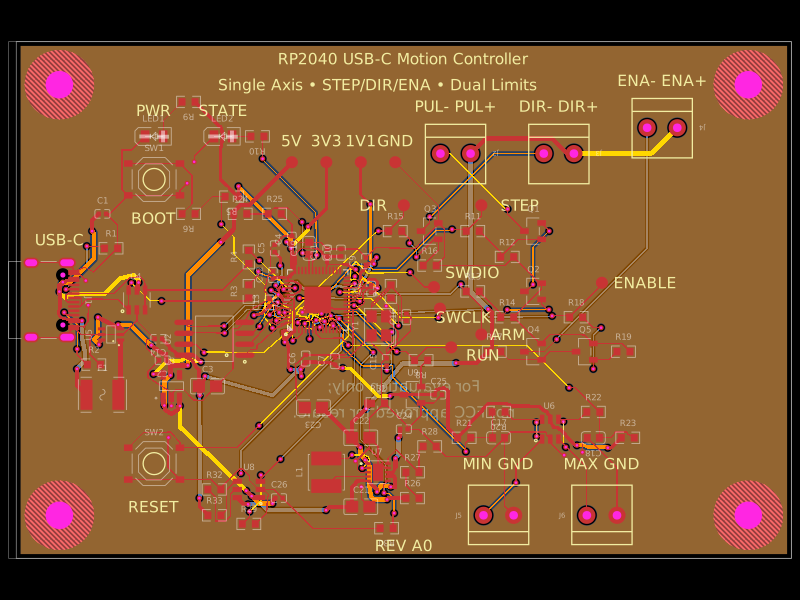 Similar packageAnasSarkiz/rp2040-usb-c-single-axis-dm542t-motion-controller--01a0e89cA USB‑C RP2040 controller board with external QSPI flash, crystal clock, regulated 3.3/1.1/5 V power, boost-converted motor-driver supply, protected USB and limit inputs, status LEDs, reset/boot switches, and AO3400A MOSFET outputs for stepper-control signals.
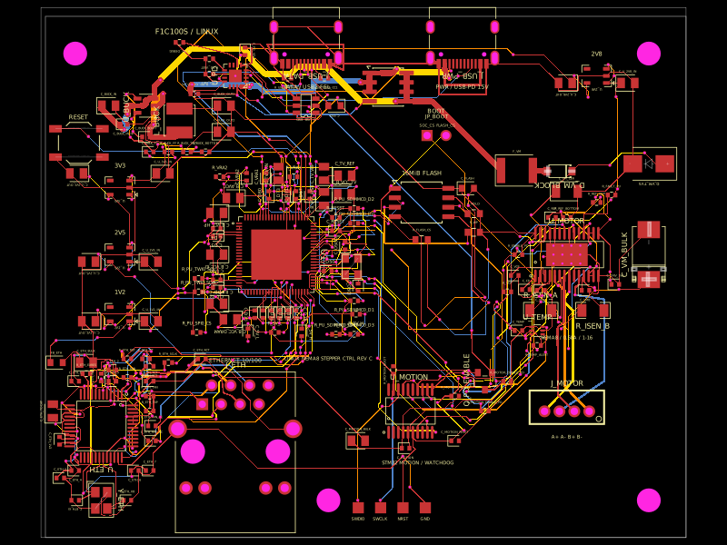 Discover something newshibosoftwaredev/f1c100s-linux-nema8-stepper-controllerA four-layer Linux motion-control carrier board combining an Allwinner F1C100S SoC, USB-C PD power, 10/100 Ethernet, STM32 watchdog-controlled DRV8825 NEMA-8 stepper drive, SPI flash, regulated power rails, USB protection, and supporting connectors/passives.