imrishabh18/nema-23-stepper-controller
A 57 mm four-layer RP2040 NEMA23 stepper-controller PCB with USB‑C/USB‑PD power input, protected motor rail, DRV8452 dual-winding driver, bidirectional current sensing, temperature/enable interlock, optional magnetic encoder, RGB LED and buzzer status indicators, and motor/test connectors.
- Version
- 1.2.3
- License
- unset
- Stars
- 0
imports/DRV8452DDWR.tsx
// EasyEDA C5624514 lands rotated +90°; retained 18 GND thermal vias and conservative courtyard.
import type { ChipProps } from "@tscircuit/props";
const pinLabels = {
    pin1: ["VCP"],
    pin2: ["VM1"],
    pin3: ["PGNDA1"],
    pin4: ["AOUT11"],
    pin5: ["AOUT12"],
    pin6: ["AOUT13"],
    pin7: ["AOUT21"],
    pin8: ["AOUT22"],
    pin9: ["AOUT23"],
    pin10: ["PGNDA2"],
    pin11: ["VM2"],
    pin12: ["VM3"],
    pin13: ["PGNDB1"],
    pin14: ["BOUT21"],
    pin15: ["BOUT22"],
    pin16: ["BOUT23"],
    pin17: ["BOUT11"],
    pin18: ["BOUT12"],
    pin19: ["BOUT13"],
    pin20: ["PGNDB2"],
    pin21: ["VM4"],
    pin22: ["GND1"],
    pin23: ["GND2"],
    pin24: ["DVDD"],
    pin25: ["VCC"],
    pin26: ["nFAULT"],
    pin27: ["nHOME"],
    pin28: ["MODE"],
    pin29: ["RSVD1"],
    pin30: ["RSVD2"],
    pin31: ["RSVD3"],
    pin32: ["RSVD4"],
    pin33: ["VREF"],
    pin34: ["nSCS"],
    pin35: ["RSVD_TOFF"],
    pin36: ["SDO"],
    pin37: ["SDI"],
    pin38: ["SCLK"],
    pin39: ["STEP"],
    pin40: ["DIR"],
    pin41: ["ENABLE"],
    pin42: ["nSLEEP"],
    pin43: ["CPL"],
    pin44: ["CPH"],
    pin45: ["EP"]
} as const;
const pinAttributes = {
    pin22: { requiresGround: true },
    pin23: { requiresGround: true },
    pin25: { requiresPower: true }
} as const;
export const DRV8452DDWR = (props: ChipProps<typeof pinLabels>) => {
    return (<chip schMarginX={0.35} schMarginY={0.7} pinLabels={pinLabels} pinAttributes={pinAttributes} supplierPartNumbers={{
            "jlcpcb": [
                "C5624514"
            ]
        }} manufacturerPartNumber="DRV8452DDWR" footprint={<footprint>
        <smtpad portHints={["pin1"]} pcbX="-6.6675mm" pcbY="-3.63753mm" width="0.308mm" height="1.575mm" shape="rect" />
        <smtpad portHints={["pin2"]} pcbX="-6.0325mm" pcbY="-3.63753mm" width="0.308mm" height="1.575mm" shape="rect" />
        <smtpad portHints={["pin3"]} pcbX="-5.3975mm" pcbY="-3.63753mm" width="0.308mm" height="1.575mm" shape="rect" />
        <smtpad portHints={["pin4"]} pcbX="-4.7625mm" pcbY="-3.63753mm" width="0.308mm" height="1.575mm" shape="rect" />
        <smtpad portHints={["pin5"]} pcbX="-4.1275mm" pcbY="-3.63753mm" width="0.308mm" height="1.575mm" shape="rect" />
        <smtpad portHints={["pin6"]} pcbX="-3.4925mm" pcbY="-3.63753mm" width="0.308mm" height="1.575mm" shape="rect" />
        <smtpad portHints={["pin7"]} pcbX="-2.8575mm" pcbY="-3.63753mm" width="0.308mm" height="1.575mm" shape="rect" />
        <smtpad portHints={["pin8"]} pcbX="-2.2225mm" pcbY="-3.63753mm" width="0.308mm" height="1.575mm" shape="rect" />
        <smtpad portHints={["pin9"]} pcbX="-1.5875mm" pcbY="-3.63753mm" width="0.308mm" height="1.575mm" shape="rect" />
        <smtpad portHints={["pin10"]} pcbX="-0.9525mm" pcbY="-3.63753mm" width="0.308mm" height="1.575mm" shape="rect" />
        <smtpad portHints={["pin11"]} pcbX="-0.3175mm" pcbY="-3.63753mm" width="0.308mm" height="1.575mm" shape="rect" />
        <smtpad portHints={["pin12"]} pcbX="0.3175mm" pcbY="-3.63753mm" width="0.308mm" height="1.575mm" shape="rect" />
        <smtpad portHints={["pin13"]} pcbX="0.9525mm" pcbY="-3.63753mm" width="0.308mm" height="1.575mm" shape="rect" />
        <smtpad portHints={["pin14"]} pcbX="1.5875mm" pcbY="-3.63753mm" width="0.308mm" height="1.575mm" shape="rect" />
        <smtpad portHints={["pin15"]} pcbX="2.2225mm" pcbY="-3.63753mm" width="0.308mm" height="1.575mm" shape="rect" />
        <smtpad portHints={["pin16"]} pcbX="2.8575mm" pcbY="-3.63753mm" width="0.308mm" height="1.575mm" shape="rect" />
        <smtpad portHints={["pin17"]} pcbX="3.4925mm" pcbY="-3.63753mm" width="0.308mm" height="1.575mm" shape="rect" />
        <smtpad portHints={["pin18"]} pcbX="4.1275mm" pcbY="-3.63753mm" width="0.308mm" height="1.575mm" shape="rect" />
        <smtpad portHints={["pin19"]} pcbX="4.7625mm" pcbY="-3.63753mm" width="0.308mm" height="1.575mm" shape="rect" />
        <smtpad portHints={["pin20"]} pcbX="5.3975mm" pcbY="-3.63753mm" width="0.308mm" height="1.575mm" shape="rect" />
        <smtpad portHints={["pin21"]} pcbX="6.0325mm" pcbY="-3.63753mm" width="0.308mm" height="1.575mm" shape="rect" />
        <smtpad portHints={["pin22"]} pcbX="6.6675mm" pcbY="-3.63753mm" width="0.308mm" height="1.575mm" shape="rect" />
        <smtpad portHints={["pin23"]} pcbX="6.6675mm" pcbY="3.63753mm" width="0.308mm" height="1.575mm" shape="rect" />
        <smtpad portHints={["pin24"]} pcbX="6.0325mm" pcbY="3.63753mm" width="0.308mm" height="1.575mm" shape="rect" />
        <smtpad portHints={["pin25"]} pcbX="5.3975mm" pcbY="3.63753mm" width="0.308mm" height="1.575mm" shape="rect" />
        <smtpad portHints={["pin26"]} pcbX="4.7625mm" pcbY="3.63753mm" width="0.308mm" height="1.575mm" shape="rect" />
        <smtpad portHints={["pin27"]} pcbX="4.1275mm" pcbY="3.63753mm" width="0.308mm" height="1.575mm" shape="rect" />
        <smtpad portHints={["pin28"]} pcbX="3.4925mm" pcbY="3.63753mm" width="0.308mm" height="1.575mm" shape="rect" />
        <smtpad portHints={["pin29"]} pcbX="2.8575mm" pcbY="3.63753mm" width="0.308mm" height="1.575mm" shape="rect" />
        <smtpad portHints={["pin30"]} pcbX="2.2225mm" pcbY="3.63753mm" width="0.308mm" height="1.575mm" shape="rect" />
        <smtpad portHints={["pin31"]} pcbX="1.5875mm" pcbY="3.63753mm" width="0.308mm" height="1.575mm" shape="rect" />
        <smtpad portHints={["pin32"]} pcbX="0.9525mm" pcbY="3.63753mm" width="0.308mm" height="1.575mm" shape="rect" />
        <smtpad portHints={["pin33"]} pcbX="0.3175mm" pcbY="3.63753mm" width="0.308mm" height="1.575mm" shape="rect" />
        <smtpad portHints={["pin34"]} pcbX="-0.3175mm" pcbY="3.63753mm" width="0.308mm" height="1.575mm" shape="rect" />
        <smtpad portHints={["pin35"]} pcbX="-0.9525mm" pcbY="3.63753mm" width="0.308mm" height="1.575mm" shape="rect" />
        <smtpad portHints={["pin36"]} pcbX="-1.5875mm" pcbY="3.63753mm" width="0.308mm" height="1.575mm" shape="rect" />
        <smtpad portHints={["pin37"]} pcbX="-2.2225mm" pcbY="3.63753mm" width="0.308mm" height="1.575mm" shape="rect" />
        <smtpad portHints={["pin38"]} pcbX="-2.8575mm" pcbY="3.63753mm" width="0.308mm" height="1.575mm" shape="rect" />
        <smtpad portHints={["pin39"]} pcbX="-3.4925mm" pcbY="3.63753mm" width="0.308mm" height="1.575mm" shape="rect" />
        <smtpad portHints={["pin40"]} pcbX="-4.1275mm" pcbY="3.63753mm" width="0.308mm" height="1.575mm" shape="rect" />
        <smtpad portHints={["pin41"]} pcbX="-4.7625mm" pcbY="3.63753mm" width="0.308mm" height="1.575mm" shape="rect" />
        <smtpad portHints={["pin42"]} pcbX="-5.3975mm" pcbY="3.63753mm" width="0.308mm" height="1.575mm" shape="rect" />
        <smtpad portHints={["pin43"]} pcbX="-6.0325mm" pcbY="3.63753mm" width="0.308mm" height="1.575mm" shape="rect" />
        <smtpad portHints={["pin44"]} pcbX="-6.6675mm" pcbY="3.63753mm" width="0.308mm" height="1.575mm" shape="rect" />
        <smtpad portHints={["pin45"]} pcbX="0mm" pcbY="0mm" width="7.59998mm" height="3.39999mm" shape="rect" />
        <via connectsTo="net.GND" pcbX="-2.499868mm" pcbY="0.999998mm" outerDiameter="0.6096mm" holeDiameter="0.3048mm" layers={["top", "bottom"]}/>
        <via connectsTo="net.GND" pcbX="-1.49987mm" pcbY="0.999998mm" outerDiameter="0.6096mm" holeDiameter="0.3048mm" layers={["top", "bottom"]}/>
        <via connectsTo="net.GND" pcbX="-0.499872mm" pcbY="0.999998mm" outerDiameter="0.6096mm" holeDiameter="0.3048mm" layers={["top", "bottom"]}/>
        <via connectsTo="net.GND" pcbX="0.500126mm" pcbY="0.999998mm" outerDiameter="0.6096mm" holeDiameter="0.3048mm" layers={["top", "bottom"]}/>
        <via connectsTo="net.GND" pcbX="1.500124mm" pcbY="0.999998mm" outerDiameter="0.6096mm" holeDiameter="0.3048mm" layers={["top", "bottom"]}/>
        <via connectsTo="net.GND" pcbX="2.500122mm" pcbY="0.999998mm" outerDiameter="0.6096mm" holeDiameter="0.3048mm" layers={["top", "bottom"]}/>
        <via connectsTo="net.GND" pcbX="2.500122mm" pcbY="0mm" outerDiameter="0.6096mm" holeDiameter="0.3048mm" layers={["top", "bottom"]}/>
        <via connectsTo="net.GND" pcbX="1.500124mm" pcbY="0mm" outerDiameter="0.6096mm" holeDiameter="0.3048mm" layers={["top", "bottom"]}/>
        <via connectsTo="net.GND" pcbX="0.500126mm" pcbY="0mm" outerDiameter="0.6096mm" holeDiameter="0.3048mm" layers={["top", "bottom"]}/>
        <via connectsTo="net.GND" pcbX="-0.499872mm" pcbY="0mm" outerDiameter="0.6096mm" holeDiameter="0.3048mm" layers={["top", "bottom"]}/>
        <via connectsTo="net.GND" pcbX="-1.49987mm" pcbY="0mm" outerDiameter="0.6096mm" holeDiameter="0.3048mm" layers={["top", "bottom"]}/>
        <via connectsTo="net.GND" pcbX="-2.499868mm" pcbY="0mm" outerDiameter="0.6096mm" holeDiameter="0.3048mm" layers={["top", "bottom"]}/>
        <via connectsTo="net.GND" pcbX="-2.499868mm" pcbY="-0.999998mm" outerDiameter="0.6096mm" holeDiameter="0.3048mm" layers={["top", "bottom"]}/>
        <via connectsTo="net.GND" pcbX="-1.49987mm" pcbY="-0.999998mm" outerDiameter="0.6096mm" holeDiameter="0.3048mm" layers={["top", "bottom"]}/>
        <via connectsTo="net.GND" pcbX="-0.499872mm" pcbY="-0.999998mm" outerDiameter="0.6096mm" holeDiameter="0.3048mm" layers={["top", "bottom"]}/>
        <via connectsTo="net.GND" pcbX="0.500126mm" pcbY="-0.999998mm" outerDiameter="0.6096mm" holeDiameter="0.3048mm" layers={["top", "bottom"]}/>
        <via connectsTo="net.GND" pcbX="1.500124mm" pcbY="-0.999998mm" outerDiameter="0.6096mm" holeDiameter="0.3048mm" layers={["top", "bottom"]}/>
        <via connectsTo="net.GND" pcbX="2.500122mm" pcbY="-0.999998mm" outerDiameter="0.6096mm" holeDiameter="0.3048mm" layers={["top", "bottom"]}/>
        <silkscreenpath route={[{ "x": -7.076211400000034, "y": -2.621406999999863 }, { "x": -7.076211400000034, "y": 2.6214069999999765 }, { "x": 7.07621139999992, "y": 2.6214069999999765 }, { "x": 7.07621139999992, "y": -2.621406999999863 }, { "x": -7.076211400000034, "y": -2.621406999999863 }]}/>
        <silkscreencircle pcbX="-6.6675mm" pcbY="-1.868932mm" radius="0.150114mm"/>
        <silkscreencircle pcbX="-7.273798mm" pcbY="-3.714496mm" radius="0.150114mm"/>
        <silkscreentext text="{NAME}" pcbX="-0.1651mm" pcbY="5.4196mm" anchorAlignment="center" fontSize="1mm"/>
        <courtyardoutline outline={[{ "x": -7.6667999999999665, "y": 4.6696000000000595 }, { "x": 7.3366000000000895, "y": 4.6696000000000595 }, { "x": 7.3366000000000895, "y": -4.847399999999993 }, { "x": -7.6667999999999665, "y": -4.847399999999993 }, { "x": -7.6667999999999665, "y": 4.6696000000000595 }]}/>
      </footprint>} cadModel={{
            objUrl: "https://modelcdn.tscircuit.com/easyeda_models/assets/C5624514.obj?uuid=8e3f11a5fbfc4e5c87265b24b564bc34",
            stepUrl: "https://modelcdn.tscircuit.com/easyeda_models/assets/C5624514.step?uuid=8e3f11a5fbfc4e5c87265b24b564bc34",
            pcbRotationOffset: 90,
            modelOriginPosition: { x: 0, y: 0, z: 0 },
        }} {...props}/>);
};
Related Packages
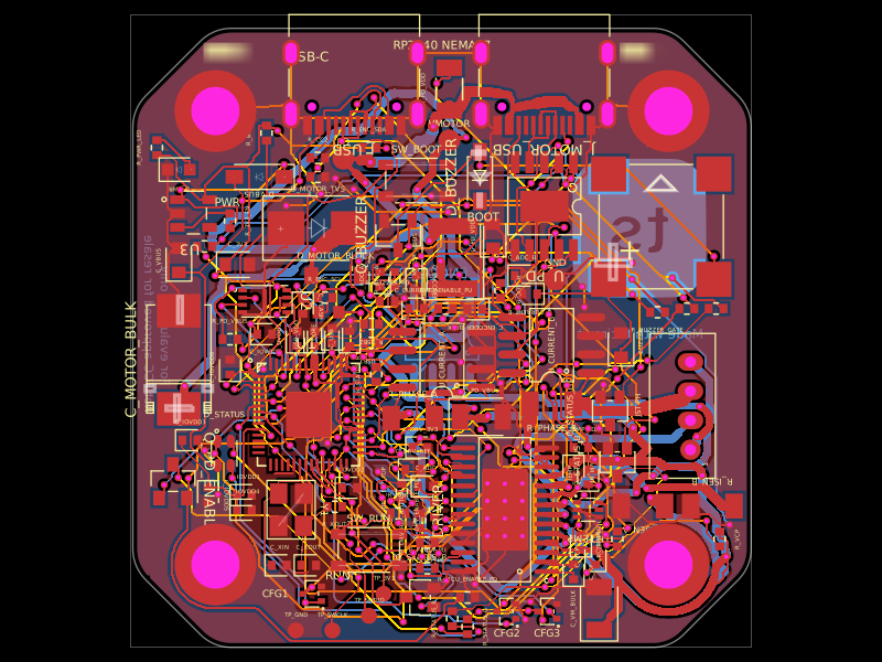 More from this authorimrishabh18/rp2040-motor-controllerA 4-layer RP2040-based USB-C/USB-PD controller board that powers and drives a NEMA17 stepper via a DRV8825, with current/temperature telemetry, RGB and buzzer status indicators, QSPI flash, protection/filtering, test points, and optional AS5600 encoder support.
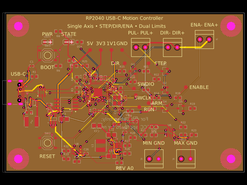 Similar packageAnasSarkiz/rp2040-usb-c-single-axis-dm542t-motion-controller--01a0e89cA USB‑C RP2040 controller board with external QSPI flash, crystal clock, regulated 3.3/1.1/5 V power, boost-converted motor-driver supply, protected USB and limit inputs, status LEDs, reset/boot switches, and AO3400A MOSFET outputs for stepper-control signals.
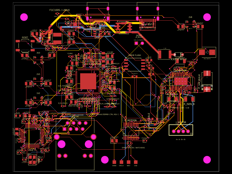 Discover something newshibosoftwaredev/f1c100s-linux-nema8-stepper-controllerA four-layer Linux motion-control carrier board combining an Allwinner F1C100S SoC, USB-C PD power, 10/100 Ethernet, STM32 watchdog-controlled DRV8825 NEMA-8 stepper drive, SPI flash, regulated power rails, USB protection, and supporting connectors/passives.