imrishabh18/nema-23-stepper-controller
A 57 mm four-layer RP2040 NEMA23 stepper-controller PCB with USB‑C/USB‑PD power input, protected motor rail, DRV8452 dual-winding driver, bidirectional current sensing, temperature/enable interlock, optional magnetic encoder, RGB LED and buzzer status indicators, and motor/test connectors.
- Version
- 1.2.3
- License
- unset
- Stars
- 0
engineering/v1.0.8-original-notes.md
# RP2040 NEMA 23 motor cap — revision C (USB-C PD + JST-XH)

> **Version 1.0.8 — not hardware-qualified.** Restores default schematic trace-distance behavior while retaining the consolidated Motor Power sheet. PCB copper is unchanged. Uses tscircuit 0.0.2642, core 0.0.1969 and schematic-trace-solver 0.0.208. The four supplier diode-polarity errors in v1.0.5 remain corrected. Supplier-enabled build, schematic analysis, PCB placement, full-build DRC and independent all-layer Gerber shorts checks pass. The build retains 44 warnings: 25 supplier footprint differences, nine unnamed traces and ten courtyard/pin-metadata warnings. See [verification.md](./verification.md); hardware, thermal and motor-fit validation are still required before fabrication/use.

Before publishing any changes, run `bun run check:release`. It includes `check:drc` and `tsci check shorts`, stops on failures (including asynchronous DRC exceptions), and records the checked source hashes in `checks/release/`.

An editable tscircuit design based on the RP2040 subsystem and two-USB-port arrangement of [the reference board](https://tscircuit.com/imrishabh18/rp2040-motor-controller). A DRV8462DDWR chopper driver and 28 V USB-C EPR input replace its low-voltage motor stage. **No screw terminals are populated.** This is an engineering prototype; the motor model and rear dimensions have not yet been supplied.

| Item | Design choice |
|---|---|
| PCB | 57 × 57 mm, four layers, 1.6 mm FR-4 |
| Copper target | 2 oz outer layers; 1 oz inner layers; confirm the fabricator can produce the fine-pitch MCU geometry with this stackup |
| Motor supply | Dedicated USB-C PD EPR port requesting 28 V; use a charger offering 28 V / 5 A on that port and a genuine EPR-rated cable |
| Input budget | Approximately 2.46 A nominal electronic limit, about 69 W at 28 V before losses; this is not the phase-current limit or a tested continuous-power rating |
| Current target | Approximately 3.00 A peak, 2.12 A RMS for sinusoidal microstepping; reduce in firmware for smaller motors |
| Logic power | Separate 5 V USB-C input; USB must remain connected to run the controller |
| Motor output | One 4-pin JST-XH B4B-XH-A(LF)(SN), 2.5 mm pitch; pins 1–4: A+, A−, B+, B− |
| Rear mounting | Four 5.2 mm unplated holes on a provisional 47.14 mm square; 8 mm screw-head copper clearances |
| Mechanical assumption | Flat rear motor face with no protruding shaft; use insulating standoffs, initially 10 mm |
| Thermal monitoring | TMP102 at 0x48 near the driver, plus an AND gate on driver ENABLE |

NEMA 23 describes the frame size, not one electrical rating. The motor's winding voltage is not the required chopper-driver supply voltage. Final supply, current, acceleration and cooling depend on winding current, inductance, speed and load. A motor marked 2.8 A must not automatically be run at 2.8 A RMS: establish the manufacturer's current convention first.

## Electrical design

Revision C replaces the power-input screw terminal with `J_USB_POWER`, a GCT USB4105-GF-A receptacle. `J_MOTOR` remains JST-XH. Its pin order matches the reference board's motor pin order, but XH is **not plug-compatible** with the smaller PH connector.

Version 1.0.4 retains tscircuit's `<connector standard="usb_c" />` schematic styling for both USB ports: signals on the right and shield contacts below. Shield contacts S1–S4 are spaced at 0.55 schematic units so their GND symbols do not overlap. VBUS labels distinguish 5 V logic power from EPR motor power. The corner GND contacts (logic pin 28 and motor-power pin 20) are identified by their physical pin numbers and external GND symbols, avoiding duplicate inner labels at the shield corner. All 16 logic-port and 20 power-port contacts remain visible and connected as before. Exact voltage-qualified footprints, PCB routing and electrical connectivity are unchanged from 1.0.2. `standard`, not the component's `name`, selects the USB-C symbol.

### USB-C power requirements

- The motor port requests **28 V EPR** using a CH224Q and a 210 kΩ configuration resistor. Ordinary 5 V USB ports and 20 V-only PD chargers do not run the motor. Do not feed 36 V or 48 V into this port. No e-marker emulation is used.
- Use a **140 W or higher EPR charger explicitly listing 28 V / 5 A on the selected port**, plus a genuine EPR-rated, electronically marked USB-C cable. A charger's total advertised wattage alone is not sufficient; multi-port sharing can remove the required profile.
- The separate USB-C programming/logic port remains **5 V only**. Both ports must be connected to operate. The two VBUS rails are distinct; only ground is shared. Never connect the 28 V motor rail to the RP2040's 5 V input.
- The reference's CH224K/9 V circuit is not copied electrically: CH224Q supply and VBUS pins connect directly to VBUS and use a 50 V bypass capacitor. Its CFG2/CFG3 pins are intentionally unused; this revision does not read the PD contract over I2C.
- The motor load stays disconnected at boot. Firmware must check active-low PD power-good, then explicitly assert `POWER_ARM`. Hardware undervoltage lockout rejects the usual 5–20 V fallback rails. Loss of PD power-good must latch off operation in firmware.

The GCT series is specified for 48 V / 5 A; the board itself is restricted to a 28 V negotiated supply. [GCT USB4105 specifications](https://gct.co/connector/usb4105). PD-controller pinout/configuration follow WCH CH224 datasheet V2.1, tables 4-1 and 5-1 and figure 6.1.1. [Manufacturer documentation](https://www.wch-ic.com/downloads/CH224DS1_PDF.html).

Use an **XHP-4** housing with **SXH-001T-P0.6** contacts and correctly crimped **22 AWG** wire. Pins 1/2 are coil A and pins 3/4 are coil B; confirm winding pairs with a meter and check the PCB's pin-1 marking rather than assuming cable colors. Do not connect or disconnect the motor while powered. The XH series is rated 3 A with 22 AWG wire; this is not permission to operate at 3 A in every thermal condition. Keep actual phase current, including reference/driver tolerances, within the connector rating and derate for the hot motor-back environment. Validate the full harness temperature rise. [JST XH manufacturer drawing and specifications](https://www.jst-mfg.com/product/pdf/eng/eXH.pdf).

The DRV8462DDWR provides integrated current sensing, STEP/DIR indexing and SPI configuration. The DDW device supports up to 5 A full-scale / 3.5 A RMS subject to thermal limits; this compact board targets less. Its external current reference is approximately 1.982 V from 3.3 V, 6.65 kΩ and 10 kΩ, corresponding to approximately 3.00 A full-scale using 0.66 V/A. SPI current scaling can reduce this value. Enabling the internal reference overrides that divider, so firmware must enforce the board's current limit. See the [TI datasheet](https://www.ti.com/lit/ds/symlink/drv8462.pdf).

The power path is USB VBUS → 4 A fuse → TPS26630RGER eFuse → SS510B blocking diode → motor rail. Only two 1 µF input capacitors precede the eFuse; the 220 µF bulk capacitor is on the controlled output. Nominal settings are 24.0 V rising UVLO, 30.36 V OVP, 2.46 A current limit (7.32 kΩ), and about 56 ms startup ramp at 28 V (100 nF dV/dt). Use 1% divider/current-limit resistors and review worst-case thresholds. MODE is left open for latched overload shutdown. PGOOD is wired with the temperature sensor's open-drain ALERT: either can inhibit the driver. [TI TPS2663 datasheet](https://www.ti.com/lit/ds/symlink/tps2663.pdf).

The retained SMBJ36A TVS, 220 µF / 63 V reservoir and 10 kΩ bleed resistor are on the motor rail. The blocking diode isolates regenerative motor energy from the USB source; the TVS is transient suppression, **not a sustained braking circuit**. High-inertia or externally driven loads need a reviewed braking/clamp solution. Raw USB VBUS/CC protection, charger interoperability, inrush and input transients still require hardware validation; this is not a USB-IF-certified design.

The driver exposed pad and power grounds connect to GND. The imported thermal-via array is explicitly assigned to GND. Four 1.2 mm motor trunks have three short 0.28 mm pin escapes each; B+ uses a bottom-layer crossover through a 0.6 mm drilled / 1.1 mm pad via to preserve the connector pin order. The motor supply has 1.5–2 mm branches. These widths are layout targets, not a tested ampacity rating. Verify temperature rise, copper thickness, via sharing and the complete return path before committing the board to production.

## Firmware interface

| Signal | RP2040 GPIO |
|---|---:|
| USB motor-power arm (eFuse SHDN, active high) | 0 |
| USB PD power-good, active low | 1 |
| eFuse fault, active low | 2 |
| SPI0 MISO / CS / SCK / MOSI | 16 / 17 / 18 / 19 |
| STEP / DIR | 20 / 21 |
| ARM request | 22 |
| Driver nFAULT | 23 |
| Combined temperature ALERT / motor power-good interlock | 24 |
| Status LED | 25 |
| I2C1 SDA / SCL | 26 / 27 |
| Driver nSLEEP (WAKE) | 28 |
| Driver nHOME | 29 |

The original DRV8847 coil-control firmware is incompatible with this driver. No executable motor firmware is supplied here. Implement these requirements before connecting a motor:

1. Keep POWER_ARM, ARM and WAKE low at boot. STEP starts low. Configure the RP2040 peripherals, leaving motor outputs disabled.
2. Configure and verify the TMP102 comparator thresholds. Initial engineering targets are warning at 65 °C, shutdown at 75 °C and re-arm only below 60 °C. These need validation against junction temperature and the actual thermal assembly.
3. With a verified 28 V / 5 A EPR source/cable, require stable PD_PG_N low, then set POWER_ARM high. Wait for the output ramp and for POWER_FAULT_N and the combined TEMP_OK/PGOOD signal to be high. Reject a timeout and latch off. A 5–20 V fallback source must never cause a motor-start attempt.
4. Drive WAKE high to communicate with the driver and wait its wake interval. Verify SPI communication/status and apply motor-specific current settings while ARM remains low. Allow ARM only after all checks pass. The gate implements `ENABLE_SAFE = ARM AND TEMP_OK`; TEMP_OK now also requires eFuse power-good.
5. Stop and latch off on loss of PD_PG_N, temperature alert, eFuse fault, communication failure or driver fault. Turn ARM and WAKE low, then POWER_ARM low. Require an explicit new arm request after the cause clears; never automatically restart after charger renegotiation. Use a watchdog; reset returns all three controls low. POWER_ARM cycling resets a latched eFuse only as part of this explicit recovery sequence.

The sensor measures PCB temperature with thermal lag. If it is missing or unpowered, its pulled-up ALERT line does not prove a safe temperature; firmware must detect that condition. Likewise the combined interlock is not a substitute for checking PD status. Removing drive also removes holding torque. No executable firmware is included; the board intentionally cannot energize the motor without implementing this startup sequence.

## Mechanical fit

Print `mounting-template.svg` at 100% and check its 20 mm calibration line with a ruler. The screw spacing is a provisional NEMA 23-sized mounting pattern, not a claim that the rear tie screws of every NEMA 23 motor match it. Measure the actual rear holes, bearing boss, cable exit and shaft clearance. Change the `mechanical` constants in `index.circuit.tsx` and recheck placement/routing if needed. Components face away from the motor. The 220 µF capacitor is approximately 25 mm tall above the PCB; include that in the enclosure envelope.

## Build

```sh
bun install --frozen-lockfile
bun run typecheck
bun run build
bun run dev
```

Use the pinned local CLI (`./node_modules/.bin/tsci`) for netlist, schematic-placement, placement and shorts checks. The CLI may exit zero while printing circuit errors, so inspect the error records as well as exit status. See `verification.md` for actual results and remaining work.

The checked routing is saved in `routing/route-plan.json`. Its input fingerprint prevents applying routes to changed PCB geometry or connectivity. To regenerate, run `bun scripts/regenerate-routing.mjs`; a failed candidate is saved in `dist/routing-draft.json` without replacing the checked plan. Always repeat all checks, including independent shorts detection, after regeneration. High-current manual paths in `power-copper.tsx` use fixed board coordinates and must be updated if their parts move. Signal routing includes 0.10 mm traces/clearances and 0.20 mm drills with 0.40 mm pads; confirm the complete stackup and annular-ring capability with the fabricator.

## Provenance and part references

- RP2040 subsystem: vendored from reference registry package v1.0.19; its MIT license is retained in `vendor/LICENSE-tscircuit-common`. The status-resistor position is adjusted for this board.
- Driver, temperature sensor and gate: exact imported package geometry; DRV8462 pin functions checked against the TI datasheet. DDV is a different pinout and is not a substitute for DDW.
- Fuse: Littelfuse 0437004.WR, 1206, 4 A / 63 V DC. [437 series datasheet](https://www.littelfuse.com/assetdocs/fuse-437-datasheet?assetguid=7efbf979-42bb-4da1-b7b4-e1ec5d2b3789).
- Bulk capacitor: Panasonic EEU-FR1J221L, 220 µF / 63 V, 10 × 25 mm, 5 mm lead pitch, 1.5 A ripple rating at 100 kHz. Verify ripple derating at the actual chopper frequency and temperature. [Manufacturer series data](https://industrial.panasonic.com/cdbs/www-data/pdf/RDF0000/ABA0000C1259.pdf).
- R_BLEED: populate a 2512 10 kΩ resistor rated at least 1 W. Populate R_REF_TOP/BOT with 1% or better parts. All VM ceramics and the flying capacitor must meet the source's voltage ratings and DC-bias requirements.

No board has been fabricated, powered or thermally characterized. Confirm the motor specification and mechanical fit, then review the complete design and perform current-limited bring-up before use.
Related Packages
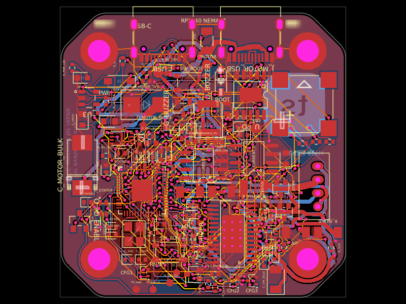 More from this authorimrishabh18/rp2040-motor-controllerA 4-layer RP2040-based USB-C/USB-PD controller board that powers and drives a NEMA17 stepper via a DRV8825, with current/temperature telemetry, RGB and buzzer status indicators, QSPI flash, protection/filtering, test points, and optional AS5600 encoder support.
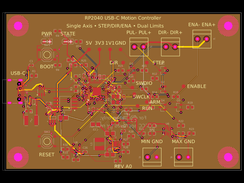 Similar packageAnasSarkiz/rp2040-usb-c-single-axis-dm542t-motion-controller--01a0e89cA USB‑C RP2040 controller board with external QSPI flash, crystal clock, regulated 3.3/1.1/5 V power, boost-converted motor-driver supply, protected USB and limit inputs, status LEDs, reset/boot switches, and AO3400A MOSFET outputs for stepper-control signals.
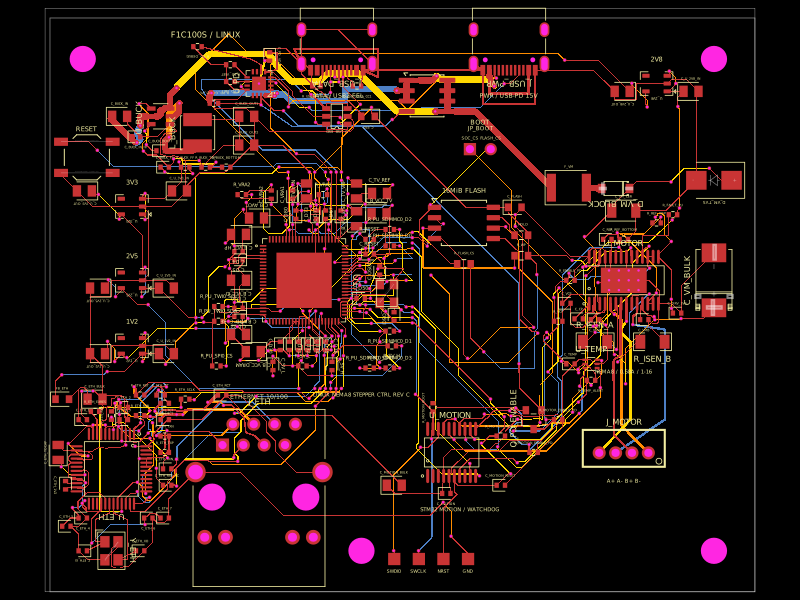 Discover something newshibosoftwaredev/f1c100s-linux-nema8-stepper-controllerA four-layer Linux motion-control carrier board combining an Allwinner F1C100S SoC, USB-C PD power, 10/100 Ethernet, STM32 watchdog-controlled DRV8825 NEMA-8 stepper drive, SPI flash, regulated power rails, USB protection, and supporting connectors/passives.