imrishabh18/fitness_watch
This code defines a React component representing an AO3400A SOT-23P surface-mount N-channel MOSFET with three pins labeled Gate (G), Source (S), and Drain (D), including electrical and physical pin configurations, schematic symbol, and associated 3D model.
- Version
- 1.0.7
- License
- unset
- Stars
- 0
index.circuit.tsx
PCB
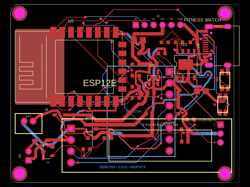
Schematic

import diodeObj from "./models/jlcpcb-C191023-1n5819ws.obj"
import switchObj from "./models/jlcpcb-C202420-switch.obj"
import usbCObj from "./models/jlcpcb-C165948-usb-c.obj"
import header1x2Obj from "./models/jlcpcb-C541856-header-1x2.obj"
import header1x3Obj from "./models/jlcpcb-C541857-header-1x3.obj"
import header1x6Obj from "./models/jlcpcb-C541860-header-1x6.obj"
import gy521Obj from "./models/gy521-module.obj"
import oledObj from "./models/ssd1306-oled-module.obj"
import resistor0603Obj from "./imports/A_0603WAF1002T5E/A_0603WAF1002T5E.obj"
import capacitor0603Obj from "./imports/CC0603KRX7R6BB105/CC0603KRX7R6BB105.obj"
import capacitor0805Obj from "./imports/FCC0805X106K100FT/FCC0805X106K100FT.obj"
import led0603Obj from "./imports/XL_1608SURC_06/XL_1608SURC_06.obj"
import pcbRoutes from "./pcb-routes.json"
import { AO3400A } from "./imports/AO3400A"
import { AO3401A } from "./imports/AO3401A"
import { AP2112K_3_3TRG1 } from "./imports/AP2112K_3_3TRG1/AP2112K_3_3TRG1"
import { B2B_PH_K_S_LF__SN_ } from "./imports/B2B_PH_K_S_LF__SN_"
import { TYPE_C_31_M_12 } from "./imports/TYPE_C_31_M_12"
import { ESP_12E } from "./imports/ESP_12E/ESP_12E"
import { TP4056 } from "./imports/TP4056/TP4056"
import { Fragment } from "react"

const USE_MANUAL_PCB_ROUTES = true

// Local copies of the exact JLCPCB package models keep the dev viewer and
// offline fabrication exports independent of the model CDN.
const jlc0603ResistorCadModel = {
  objUrl: resistor0603Obj,
  pcbRotationOffset: 90,
  modelOriginPosition: { x: -0.005, y: 0, z: -0.01 },
} as const

const jlc0603CapacitorCadModel = {
  objUrl: capacitor0603Obj,
  pcbRotationOffset: 0,
  modelOriginPosition: { x: 0, y: 0, z: -0.4 },
} as const

const jlc0805CapacitorCadModel = {
  objUrl: capacitor0805Obj,
  pcbRotationOffset: 0,
  modelOriginPosition: { x: 0, y: -0.0000127, z: -0.65 },
} as const

const jlc0603LedCadModel = {
  objUrl: led0603Obj,
  pcbRotationOffset: 0,
  modelOriginPosition: { x: -0.0000127, y: 0.0000508, z: -0.01 },
} as const

const toAnchorLocalPoint = (
  point: { x: number; y: number },
  anchor: { x: number; y: number; rotation: number; layer: string },
) => {
  const radians = (anchor.rotation * Math.PI) / 180
  const dx = point.x - anchor.x
  const dy = point.y - anchor.y
  const x = Math.cos(radians) * dx + Math.sin(radians) * dy
  const y = -Math.sin(radians) * dx + Math.cos(radians) * dy

  return { x, y }
}

const ManualPcbRouting = () => (
  <>
    {pcbRoutes.pcbTraces.map((trace, index) => {
      const firstPoint = trace.route[0]
      const lastPoint = trace.route[trace.route.length - 1]
      const getPointPosition = (point: (typeof trace.route)[number]) =>
        ({ x: point.x as number, y: point.y as number })
      const firstPosition = getPointPosition(firstPoint)
      const lastPosition = getPointPosition(lastPoint)
      const sameAsEndpoint = (point: (typeof trace.route)[number]) => {
        const position = getPointPosition(point)
        return (
          (position.x === firstPosition.x && position.y === firstPosition.y) ||
          (position.x === lastPosition.x && position.y === lastPosition.y)
        )
      }
      const pcbPath = trace.route
        .slice(1, -1)
        .filter(
          (point) => point.route_type === "via" || !sameAsEndpoint(point),
        )
        .map((point, interiorIndex) => {
          const localPoint = toAnchorLocalPoint(
            getPointPosition(point),
            trace.anchor,
          )
          if (point.route_type === "via") {
            const routeIndex = interiorIndex + 1
            const previousWire = [...trace.route.slice(0, routeIndex)]
              .reverse()
              .find((candidate) => candidate.route_type === "wire")
            const nextWire = trace.route
              .slice(routeIndex + 1)
              .find((candidate) => candidate.route_type === "wire")
            return {
              ...localPoint,
              via: true,
              fromLayer: previousWire?.layer,
              toLayer: nextWire?.layer,
            }
          }
          return localPoint
        })
      const routeWidth = Math.min(
        ...trace.route
          .filter((point) => point.route_type === "wire")
          .map((point) => Number(point.width ?? 0.15)),
      )

      return (
        <Fragment key={`manual-route-${index}`}>
        <trace
          name={`ROUTE_${index.toString().padStart(3, "0")}`}
          from={trace.from}
          to={trace.to}
          width={routeWidth}
          pcbPathRelativeTo={trace.from}
          pcbPath={pcbPath as any}
        />
        </Fragment>
      )
    })}
  </>
)

const oledPinLabels = {
  pin1: "GND",
  pin2: "VCC",
  pin3: "SCL",
  pin4: "SDA",
} as const

const mpu6050PinLabels = {
  pin1: "VCC",
  pin2: "GND",
  pin3: "SCL",
  pin4: "SDA",
  pin5: "XDA",
  pin6: "XCL",
  pin7: "AD0",
  pin8: "INT",
} as const

const OledModuleFootprint = () => (
  <footprint originalLayer="top">
    {/* The display board is socketed above the PCB, so its assembly courtyard
        covers the four-pin header only. The full module outline remains on
        silkscreen for enclosure and spacer verification. */}
    <courtyardrect pcbX="-17mm" pcbY={0} width="2.4mm" height="10.2mm" />
    <silkscreenrect
      pcbX={0}
      pcbY={0}
      width="38mm"
      height="12mm"
      filled={false}
      stroke="solid"
      strokeWidth="0.2mm"
    />
    <silkscreenrect
      pcbX="3mm"
      pcbY={0}
      width="23mm"
      height="7mm"
      filled={false}
      stroke="solid"
      strokeWidth="0.15mm"
    />
    <silkscreentext
      text="0.91in OLED / SSD1306"
      pcbX="3mm"
      pcbY="4.7mm"
      fontSize="0.7mm"
    />
    <platedhole
      shape="circular_hole_with_rect_pad"
      holeDiameter="1mm"
      rectPadWidth="1.8mm"
      rectPadHeight="1.8mm"
      pcbX="-17mm"
      pcbY="3.81mm"
      portHints={["pin1"]}
    />
    <platedhole
      shape="circle"
      holeDiameter="1mm"
      outerDiameter="1.8mm"
      pcbX="-17mm"
      pcbY="1.27mm"
      portHints={["pin2"]}
    />
    <platedhole
      shape="circle"
      holeDiameter="1mm"
      outerDiameter="1.8mm"
      pcbX="-17mm"
      pcbY="-1.27mm"
      portHints={["pin3"]}
    />
    <platedhole
      shape="circle"
      holeDiameter="1mm"
      outerDiameter="1.8mm"
      pcbX="-17mm"
      pcbY="-3.81mm"
      portHints={["pin4"]}
    />
  </footprint>
)

const Mpu6050Pin = ({ index }: { index: number }) => {
  const commonProps = {
    holeDiameter: "1mm",
    pcbX: "-6.35mm",
    pcbY: `${8.89 - index * 2.54}mm`,
    portHints: [`pin${index + 1}`],
  }

  if (index === 0) {
    return (
      <platedhole
        shape="circular_hole_with_rect_pad"
        rectPadWidth="1.8mm"
        rectPadHeight="1.8mm"
        {...commonProps}
      />
    )
  }

  return <platedhole shape="circle" outerDiameter="1.8mm" {...commonProps} />
}

const Mpu6050ModuleFootprint = () => (
  <footprint originalLayer="top">
    <courtyardrect pcbX={0} pcbY={0} width="15.7mm" height="20.8mm" />
    <silkscreenrect
      pcbX={0}
      pcbY={0}
      width="15.2mm"
      height="20.3mm"
      filled={false}
      stroke="solid"
      strokeWidth="0.2mm"
    />
    <silkscreentext
      text="MPU6050"
      pcbX="1.6mm"
      pcbY={0}
      fontSize="0.8mm"
    />
    {Array.from({ length: 8 }, (_, index) => (
      <Mpu6050Pin key={`mpu6050-pin-${index + 1}`} index={index} />
    ))}
  </footprint>
)

const Jlc0603ResistorFootprint = () => (
  <footprint originalLayer="top">
    <courtyardrect pcbX={0} pcbY={0} width="2.5mm" height="1.1mm" />
    <smtpad shape="rect" width="0.8064754mm" height="0.8640064mm" pcbX="-0.753364mm" pcbY={0} portHints={["pin1"]} />
    <smtpad shape="rect" width="0.8064754mm" height="0.8640064mm" pcbX="0.753364mm" pcbY={0} portHints={["pin2"]} />
  </footprint>
)

const Jlc0603CapacitorFootprint = () => (
  <footprint originalLayer="top">
    <courtyardrect pcbX={0} pcbY={0} width="2.5mm" height="1.2mm" />
    <smtpad shape="rect" width="0.7999984mm" height="0.8999982mm" pcbX="-0.700024mm" pcbY={0} portHints={["pin1"]} />
    <smtpad shape="rect" width="0.7999984mm" height="0.8999982mm" pcbX="0.700024mm" pcbY={0} portHints={["pin2"]} />
  </footprint>
)

const Jlc0805CapacitorFootprint = () => (
  <footprint originalLayer="top">
    <courtyardrect pcbX={0} pcbY={0} width="3.7mm" height="1.65mm" />
    <smtpad shape="rect" width="1.4100048mm" height="1.35001mm" pcbX="-0.999998mm" pcbY={0} portHints={["pin1"]} />
    <smtpad shape="rect" width="1.4100048mm" height="1.35001mm" pcbX="0.999998mm" pcbY={0} portHints={["pin2"]} />
  </footprint>
)

const JlcLedC965799Footprint = () => (
  <footprint originalLayer="top">
    <courtyardrect pcbX={0} pcbY={0} width="2.8mm" height="1.3mm" />
    <smtpad
      shape="rect"
      width="0.8mm"
      height="0.8mm"
      pcbX="-0.749mm"
      pcbY={0}
      portHints={["pin1"]}
    />
    <smtpad
      shape="rect"
      width="0.8mm"
      height="0.8mm"
      pcbX="0.749mm"
      pcbY={0}
      portHints={["pin2"]}
    />
  </footprint>
)

const JlcDiodeC191023Footprint = () => (
  <footprint originalLayer="top">
    <courtyardrect pcbX={0} pcbY={0} width="3.85mm" height="1.3mm" />
    <smtpad
      shape="rect"
      width="1mm"
      height="0.7mm"
      pcbX="-1.172464mm"
      pcbY={0}
      portHints={["pin1"]}
    />
    <smtpad
      shape="rect"
      width="1mm"
      height="0.7mm"
      pcbX="1.172464mm"
      pcbY={0}
      portHints={["pin2"]}
    />
  </footprint>
)

const JlcSwitchC202420Footprint = () => (
  <footprint originalLayer="top">
    <courtyardrect pcbX={0} pcbY={0} width="5.0002mm" height="3.1501mm" />
    <smtpad shape="rect" width="1.4mm" height="0.9mm" pcbX="-1.800098mm" pcbY="-1.125042mm" portHints={["pin1"]} />
    <smtpad shape="rect" width="1.4mm" height="0.9mm" pcbX="1.800098mm" pcbY="-1.125042mm" portHints={["pin2"]} />
    <smtpad shape="rect" width="1.4mm" height="0.9mm" pcbX="-1.800098mm" pcbY="0.17493mm" portHints={["pin3"]} />
    <smtpad shape="rect" width="1.4mm" height="0.9mm" pcbX="1.800098mm" pcbY="0.17493mm" portHints={["pin4"]} />
    <smtpad shape="rect" width="0.6mm" height="0.5mm" pcbX={0} pcbY="1.325042mm" portHints={["pin5"]} />
    <silkscreenrect
      pcbX={0}
      pcbY="-0.475mm"
      width="3.5mm"
      height="2.2mm"
      filled={false}
      stroke="solid"
      strokeWidth="0.2mm"
    />
  </footprint>
)

const JstPh2BatteryFootprint = () => (
  <footprint originalLayer="top">
    <courtyardrect pcbX={0} pcbY="-0.55mm" width="6.5mm" height="5mm" />
    {/* C131337 identifies pin 1 on the right when viewed from the top. */}
    <platedhole shape="circle" holeDiameter="0.9mm" outerDiameter="1.6mm" pcbX="1mm" pcbY={0} portHints={["pin1"]} />
    <platedhole shape="circle" holeDiameter="0.9mm" outerDiameter="1.6mm" pcbX="-1mm" pcbY={0} portHints={["pin2"]} />
    <silkscreenrect pcbX={0} pcbY="-0.55mm" width="6mm" height="4.5mm" filled={false} stroke="solid" strokeWidth="0.2mm" />
    <silkscreentext text="BAT" pcbX={0} pcbY="1.1mm" fontSize="0.6mm" />
  </footprint>
)

export default () => (
  <board
    title="ESP8266 Fitness Watch"
    width="50mm"
    height="40mm"
    thickness="1.6mm"
    borderRadius="2mm"
    layers={2}
    solderMaskColor="black"
    silkscreenColor="white"
    doubleSidedAssembly
    routingDisabled={USE_MANUAL_PCB_ROUTES}
    pcbStyle={{ viaPadDiameter: "0.6mm", viaHoleDiameter: "0.3mm" }}
  >
    <net name="GND" isGroundNet />
    <net name="VBUS" />
    <net name="VBAT" />
    <net name="VSYS" />
    <net name="V3V3" />
    <net name="I2C_SCL" />
    <net name="I2C_SDA" />
    <net name="MOTOR_LOW" />
    <net name="PULSE_RAW" />
    <net name="PULSE_ADC" />

    {/* Four non-plated M2-class band/case mounting holes on dedicated
        upper and lower side rails. A 1.7 mm keepout radius provides 0.5 mm
        copper clearance around each 2.4 mm drill on both layers. */}
    <hole name="H1" diameter="2.4mm" pcbX={-23} pcbY={18} />
    <hole name="H2" diameter="2.4mm" pcbX={23} pcbY={18} />
    <hole name="H3" diameter="2.4mm" pcbX={-23} pcbY={-18} />
    <hole name="H4" diameter="2.4mm" pcbX={23} pcbY={-18} />
    <keepout shape="circle" radius="1.7mm" pcbX={-23} pcbY={18} layers={["top", "bottom"]} />
    <keepout shape="circle" radius="1.7mm" pcbX={23} pcbY={18} layers={["top", "bottom"]} />
    <keepout shape="circle" radius="1.7mm" pcbX={-23} pcbY={-18} layers={["top", "bottom"]} />
    <keepout shape="circle" radius="1.7mm" pcbX={23} pcbY={-18} layers={["top", "bottom"]} />

    {/* Functional schematic regions. Cross-section nets are rendered as
        labeled connections, keeping each block compact and readable. */}
    <schematicsection name="charging" displayName="USB-C & LiPo Charging" sectionTitleFontSize="0.34mm" />
    <schematicsection name="regulation" displayName="Battery & 3.3 V Regulation" sectionTitleFontSize="0.34mm" />
    <schematicsection name="controller" displayName="ESP8266 Core, Controls & Motor" sectionTitleFontSize="0.34mm" />
    <schematicsection name="peripherals" displayName="Display, Motion & Pulse Sensors" sectionTitleFontSize="0.34mm" />

    {USE_MANUAL_PCB_ROUTES && <ManualPcbRouting />}

    {/*
      Source-owned manual routing. These traces are generated from the verified
      CLI autorouter result and associated with their stable source trace IDs,
      so the TSX dev view and fabrication build use identical copper geometry.
    */}
    {/* ESP8266 core. The antenna faces the left edge, with copper kept away. */}
    <ESP_12E
      name="U2"
      manufacturerPartNumber="ESP-12E"
      pcbX={-7.625}
      pcbY={6}
      pcbRotation={0}
      schSectionName="controller"
      schX={-7.5}
      schY={-2.5}
      schWidth="4mm"
      schHeight="6mm"
      schPinStyle={{
        ADC: { marginTop: "0.14mm" },
        EN: { marginTop: "0.14mm" },
        GPIO16: { marginTop: "0.14mm" },
        GPIO14: { marginTop: "0.14mm" },
        GPIO12: { marginTop: "0.14mm" },
        GPIO13: { marginTop: "0.14mm" },
        VCC: { marginTop: "0.14mm" },
        RXD: { marginTop: "0.14mm" },
        GPIO5: { marginTop: "0.14mm" },
        GPIO4: { marginTop: "0.14mm" },
        GPIO0: { marginTop: "0.14mm" },
        GPIO2: { marginTop: "0.14mm" },
        GPIO15: { marginTop: "0.14mm" },
        GND: { marginTop: "0.14mm" },
        MISO: { marginLeft: "0.14mm" },
        GPIO9: { marginLeft: "0.14mm" },
        GPIO10: { marginLeft: "0.14mm" },
        MOSI: { marginLeft: "0.14mm" },
        SCLK: { marginLeft: "0.14mm" },
      }}
      schPinArrangement={{
        leftSide: [
          "RESET",
          "ADC",
          "EN",
          "GPIO16",
          "GPIO14",
          "GPIO12",
          "GPIO13",
          "VCC",
        ],
        rightSide: [
          "TXD",
          "RXD",
          "GPIO5",
          "GPIO4",
          "GPIO0",
          "GPIO2",
          "GPIO15",
          "GND",
        ],
        bottomSide: ["CS0", "MISO", "GPIO9", "GPIO10", "MOSI", "SCLK"],
      }}
      noConnect={[
        "GPIO16",
        "GPIO12",
        "GPIO13",
        "CS0",
        "MISO",
        "GPIO9",
        "GPIO10",
        "MOSI",
        "SCLK",
      ]}
    />
    <keepout
      shape="rect"
      pcbX={-18.5}
      pcbY={6}
      width="11mm"
      height="17mm"
      layers={["top", "bottom"]}
      excludeRefs={[".U2"]}
    />

    {/* USB-C input and TP4056 LiPo charging block. */}
    <TYPE_C_31_M_12
      name="J3"
      cadModel={{
        objUrl: usbCObj,
        pcbRotationOffset: 180,
        modelOriginPosition: { x: 0, y: -2.7500289000000517, z: 0.000010999999999872223 },
      }}
      pcbX="20.8mm"
      pcbY="10.7mm"
      pcbRotation={90}
      schSectionName="charging"
      schX={-13}
      schY={11}
      schWidth="3.6mm"
      schHeight="4.2mm"
      schPinStyle={{
        A4B9: { marginTop: "0.15mm" },
        A5: { marginTop: "0.22mm" },
        B5: { marginTop: "0.15mm" },
        B1A12: { marginTop: "0.15mm" },
        EH1: { marginTop: "0.22mm" },
        EH2: { marginTop: "0.15mm" },
        EH3: { marginTop: "0.15mm" },
        EH4: { marginTop: "0.15mm" },
        B6: { marginLeft: "0.15mm" },
        A7: { marginLeft: "0.15mm" },
        B7: { marginLeft: "0.15mm" },
        A8: { marginLeft: "0.15mm" },
        B8: { marginLeft: "0.15mm" },
      }}
      schPinArrangement={{
        leftSide: ["B4A9", "A4B9", "A5", "B5"],
        rightSide: ["A1B12", "B1A12", "EH1", "EH2", "EH3", "EH4"],
        bottomSide: ["A6", "B6", "A7", "B7", "A8", "B8"],
      }}
      noConnect={["A6", "B6", "A7", "B7", "A8", "B8"]}
    />
    <TP4056
      name="U3"
      pcbX="14.2mm"
      pcbY="6.5mm"
      schSectionName="charging"
      schX={-7}
      schY={11}
      schWidth="3.1mm"
      schHeight="3.3mm"
      schPinStyle={{
        PROG: { marginTop: "0.18mm" },
        GND: { marginTop: "0.18mm" },
        VCC: { marginTop: "0.18mm" },
        CHRG: { marginTop: "0.18mm" },
        STDBY: { marginTop: "0.18mm" },
        BAT: { marginTop: "0.18mm" },
      }}
      schPinArrangement={{
        leftSide: ["TEMP", "PROG", "GND", "VCC"],
        rightSide: ["CE", "CHRG", "STDBY", "BAT"],
      }}
      noConnect={["STDBY"]}
    />
    <resistor name="R1" resistance="10k" manufacturerPartNumber="0603WAF1002T5E" supplierPartNumbers={{ jlcpcb: ["C25804"] }} footprint={<Jlc0603ResistorFootprint />} cadModel={jlc0603ResistorCadModel} pcbX="8.8mm" pcbY="9mm" schSectionName="charging" schX={-7.5} schY={6.5} schRotation={90} />
    <resistor name="R2" resistance="1k" manufacturerPartNumber="0603WAF1001T5E" supplierPartNumbers={{ jlcpcb: ["C21190"] }} footprint={<Jlc0603ResistorFootprint />} cadModel={jlc0603ResistorCadModel} pcbX="12.7mm" pcbY="11.5mm" schSectionName="charging" schX={-5} schY={15.5} />
    <led
      name="D1"
      color="red"
      manufacturerPartNumber="XL-1608SURC-06"
      supplierPartNumbers={{ jlcpcb: ["C965799"] }}
      footprint={<JlcLedC965799Footprint />}
      cadModel={jlc0603LedCadModel}
      pinLabels={{ pin1: "CATHODE", pin2: "ANODE" }}
      pcbX="9.5mm"
      pcbY="11.5mm"
      pcbRotation={180}
      schSectionName="charging"
      schX={-8}
      schY={15.5}
    />
    <capacitor name="C1" capacitance="10uF" manufacturerPartNumber="FCC0805X106K100FT" supplierPartNumbers={{ jlcpcb: ["C5137471"] }} footprint={<Jlc0805CapacitorFootprint />} cadModel={jlc0805CapacitorCadModel} pcbX="17.7mm" pcbY="0.5mm" schSectionName="charging" schX={-11} schY={7.5} schRotation={90} />
    <capacitor name="C2" capacitance="1uF" manufacturerPartNumber="CC0603KRX7R6BB105" supplierPartNumbers={{ jlcpcb: ["C113807"] }} footprint={<Jlc0603CapacitorFootprint />} cadModel={jlc0603CapacitorCadModel} pcbX="6mm" pcbY="-4.5mm" schSectionName="charging" schX={-3} schY={7.5} schRotation={90} />
    <resistor name="R10" resistance="5.1k" manufacturerPartNumber="0603WAF5101T5E" supplierPartNumbers={{ jlcpcb: ["C23186"] }} footprint={<Jlc0603ResistorFootprint />} cadModel={jlc0603ResistorCadModel} pcbX="12.5mm" pcbY="-3.8mm" pcbRotation={90} schSectionName="charging" schX={-15} schY={7} schRotation={90} />
    <resistor name="R11" resistance="5.1k" manufacturerPartNumber="0603WAF5101T5E" supplierPartNumbers={{ jlcpcb: ["C23186"] }} footprint={<Jlc0603ResistorFootprint />} cadModel={jlc0603ResistorCadModel} pcbX="16mm" pcbY="11.5mm" schSectionName="charging" schX={-12.5} schY={7} schRotation={90} />

    {/* USB/battery load sharing: USB powers VSYS while charging and Q2
        automatically isolates the cell. With USB absent, Q2 connects the
        battery to VSYS with only its low channel resistance. */}
    <AO3401A
      name="Q2"
      pcbX="-7mm"
      pcbY="-7mm"
      schSectionName="charging"
      schX={-2}
      schY={11}
    />
    <diode
      name="D3"
      variant="schottky"
      manufacturerPartNumber="1N5819WS"
      supplierPartNumbers={{ jlcpcb: ["C191023"] }}
      footprint={<JlcDiodeC191023Footprint />}
      pinLabels={{ pin1: "CATHODE", pin2: "ANODE" }}
      cadModel={{ objUrl: diodeObj, modelOriginPosition: { x: 0, y: 0.00011430000006384944, z: 0 } }}
      pcbX="-14mm"
      pcbY="-4.8mm"
      pcbRotation={180}
      schSectionName="charging"
      schX={0}
      schY={11}
    />
    <resistor name="R12" resistance="100k" manufacturerPartNumber="0603WAF1003T5E" supplierPartNumbers={{ jlcpcb: ["C25803"] }} footprint={<Jlc0603ResistorFootprint />} cadModel={jlc0603ResistorCadModel} pcbX="-7mm" pcbY="-10mm" schSectionName="charging" schX={1} schY={8} schRotation={90} />

    {/* Battery input and 600 mA AP2112K 3.3 V regulator. */}
    <B2B_PH_K_S_LF__SN_
      name="J1"
      footprint={<JstPh2BatteryFootprint />}
      pcbX="-21mm"
      pcbY="-6.2mm"
      pcbRotation={0}
      schSectionName="regulation"
      schX={16}
      schY={11}
      schWidth="2.3mm"
      schHeight="1.7mm"
    />
    <AP2112K_3_3TRG1
      name="U1"
      pcbX="7mm"
      pcbY="3.5mm"
      schSectionName="regulation"
      schX={8}
      schY={11}
      schWidth="2.8mm"
      schHeight="2.1mm"
      schPinStyle={{ GND: { marginTop: "0.2mm" } }}
      schPinArrangement={{ leftSide: ["VIN", "GND", "EN"], rightSide: ["VOUT", "NC"] }}
      noConnect={["NC"]}
    />
    <capacitor name="C3" capacitance="1uF" manufacturerPartNumber="CC0603KRX7R6BB105" supplierPartNumbers={{ jlcpcb: ["C113807"] }} footprint={<Jlc0603CapacitorFootprint />} cadModel={jlc0603CapacitorCadModel} pcbX="6.4mm" pcbY="0.2mm" schSectionName="regulation" schX={5.5} schY={8} schRotation={90} />
    <capacitor name="C4" capacitance="1uF" manufacturerPartNumber="CC0603KRX7R6BB105" supplierPartNumbers={{ jlcpcb: ["C113807"] }} footprint={<Jlc0603CapacitorFootprint />} cadModel={jlc0603CapacitorCadModel} pcbX="7mm" pcbY="6.7mm" schSectionName="regulation" schX={10.5} schY={8} schRotation={90} />

    {/* Boot straps and user controls. */}
    <resistor name="R3" resistance="10k" manufacturerPartNumber="0603WAF1002T5E" supplierPartNumbers={{ jlcpcb: ["C25804"] }} footprint={<Jlc0603ResistorFootprint />} cadModel={jlc0603ResistorCadModel} pcbX="3mm" pcbY="6.5mm" schSectionName="controller" schX={-11.5} schY={-1} schRotation={90} />
    <resistor name="R4" resistance="10k" manufacturerPartNumber="0603WAF1002T5E" supplierPartNumbers={{ jlcpcb: ["C25804"] }} footprint={<Jlc0603ResistorFootprint />} cadModel={jlc0603ResistorCadModel} pcbX="3mm" pcbY="4mm" schSectionName="controller" schX={-3.7} schY={-4.5} schRotation={90} />
    <resistor name="R5" resistance="10k" manufacturerPartNumber="0603WAF1002T5E" supplierPartNumbers={{ jlcpcb: ["C25804"] }} footprint={<Jlc0603ResistorFootprint />} cadModel={jlc0603ResistorCadModel} pcbX="3mm" pcbY="1.5mm" schSectionName="controller" schX={-3.7} schY={-2.5} schRotation={90} />
    <resistor name="R6" resistance="10k" manufacturerPartNumber="0603WAF1002T5E" supplierPartNumbers={{ jlcpcb: ["C25804"] }} footprint={<Jlc0603ResistorFootprint />} cadModel={jlc0603ResistorCadModel} pcbX="3mm" pcbY="-1mm" schSectionName="controller" schX={-11.5} schY={-3} schRotation={90} />
    <pushbutton
      name="SW_RST"
      manufacturerPartNumber="SKSCPCE010"
      supplierPartNumbers={{ jlcpcb: ["C202420"] }}
      footprint={<JlcSwitchC202420Footprint />}
      cadModel={{
        objUrl: switchObj,
        // Center the C202420 body between the two custom footprint pads.
        modelOriginPosition: { x: 0, y: -0.17500000000000004, z: -0.01 },
      }}
      pinLabels={{ pin1: "RESET", pin2: "GND", pin3: "NC3", pin4: "NC4", pin5: "SHIELD" }}
      noConnect={["NC3", "NC4", "SHIELD"]}
      pcbX="22.5mm"
      pcbY="3mm"
      pcbRotation={90}
      schSectionName="controller"
      schX={-14}
      schY={-5}
    />
    <pushbutton
      name="SW_NAV"
      manufacturerPartNumber="SKSCPCE010"
      supplierPartNumbers={{ jlcpcb: ["C202420"] }}
      footprint={<JlcSwitchC202420Footprint />}
      cadModel={{
        objUrl: switchObj,
        // Center the C202420 body between the two custom footprint pads.
        modelOriginPosition: { x: 0, y: -0.17500000000000004, z: -0.01 },
      }}
      pinLabels={{ pin1: "GPIO0", pin2: "GND", pin3: "NC3", pin4: "NC4", pin5: "SHIELD" }}
      noConnect={["NC3", "NC4", "SHIELD"]}
      pcbX="22mm"
      pcbY="-2.5mm"
      pcbRotation={90}
      schSectionName="controller"
      schX={-4}
      schY={-7}
    />

    {/* Display and motion-sensor daughterboard headers. */}
    <chip
      name="DS1"
      manufacturerPartNumber="SSD1306-128x32-I2C-module"
      footprint={<OledModuleFootprint />}
      cadModel={{
        objUrl: oledObj,
        modelOriginPosition: { x: 0, y: 0, z: 0 },
        positionOffset: { x: 17, y: 0, z: 0 },
      }}
      pinLabels={oledPinLabels}
      pinAttributes={{ pin1: { requiresGround: true }, pin2: { requiresPower: true } }}
      pcbX="5.5mm"
      pcbY="-11.7mm"
      schSectionName="peripherals"
      schX={13}
      schY={2}
      schWidth="2.8mm"
      schHeight="2.7mm"
      schPinStyle={{
        VCC: { marginTop: "0.18mm" },
        SCL: { marginTop: "0.18mm" },
        SDA: { marginTop: "0.18mm" },
      }}
      schPinArrangement={{ leftSide: ["GND", "VCC", "SCL", "SDA"] }}
    />
    <chip
      name="U4"
      manufacturerPartNumber="GY-521-MPU6050-module"
      footprint={<Mpu6050ModuleFootprint />}
      cadModel={{
        objUrl: gy521Obj,
        modelOriginPosition: { x: 0, y: 0, z: 0 },
        positionOffset: { x: -6.35, y: 0, z: 0 },
      }}
      pinLabels={mpu6050PinLabels}
      pinAttributes={{ pin1: { requiresPower: true }, pin2: { requiresGround: true } }}
      layer="bottom"
      pcbX="4.2mm"
      pcbY="-4mm"
      pcbRotation={0}
      schSectionName="peripherals"
      schX={13}
      schY={-5}
      schWidth="3mm"
      schHeight="4.8mm"
      schPinStyle={{
        GND: { marginTop: "0.14mm" },
        SCL: { marginTop: "0.14mm" },
        SDA: { marginTop: "0.14mm" },
        XDA: { marginTop: "0.14mm" },
        XCL: { marginTop: "0.14mm" },
        AD0: { marginTop: "0.14mm" },
        INT: { marginTop: "0.14mm" },
      }}
      schPinArrangement={{ leftSide: ["VCC", "GND", "SCL", "SDA", "XDA", "XCL", "AD0", "INT"] }}
      noConnect={["XDA", "XCL", "AD0", "INT"]}
    />

    {/* Reference firmware uses ADC0 for pulse graphing; this header makes it explicit. */}
    <pinheader
      name="J4"
      manufacturerPartNumber="PZ200V-11-03P"
      supplierPartNumbers={{ jlcpcb: ["C541857"] }}
      cadModel={{
        objUrl: header1x3Obj,
        modelOriginPosition: { x: 0, y: 0, z: 0.19999400000000023 },
      }}
      pinCount={3}
      pitch="2mm"
      gender="male"
      rightAngle
      pinLabels={["PULSE_VCC", "PULSE_GND", "PULSE_SIG"]}
      pcbPinLabels={{ pin1: "3V3", pin2: "GND", pin3: "SIG" }}
      showSilkscreenPinLabels
      layer="bottom"
      pcbX="22mm"
      pcbY="-9mm"
      pcbRotation={90}
      schSectionName="peripherals"
      schX={8}
      schY={-11}
      schWidth="2.4mm"
      schHeight="2.1mm"
      schPinStyle={{
        PULSE_GND: { marginTop: "0.18mm" },
        PULSE_SIG: { marginTop: "0.18mm" },
      }}
    />
    <resistor name="R7" resistance="270k" manufacturerPartNumber="0603WAF2703T5E" supplierPartNumbers={{ jlcpcb: ["C22965"] }} footprint={<Jlc0603ResistorFootprint />} cadModel={jlc0603ResistorCadModel} pcbX="15.2mm" pcbY="-5.8mm" schSectionName="peripherals" schX={11.5} schY={-11} />
    <resistor name="R8" resistance="100k" manufacturerPartNumber="0603WAF1003T5E" supplierPartNumbers={{ jlcpcb: ["C25803"] }} footprint={<Jlc0603ResistorFootprint />} cadModel={jlc0603ResistorCadModel} pcbX="14mm" pcbY="-8mm" schSectionName="peripherals" schX={14.5} schY={-13.5} schRotation={90} />
    <capacitor name="C5" capacitance="100nF" manufacturerPartNumber="CC0603KRX7R9BB104" supplierPartNumbers={{ jlcpcb: ["C14663"] }} footprint={<Jlc0603CapacitorFootprint />} cadModel={jlc0603CapacitorCadModel} pcbX="14mm" pcbY="-10.8mm" schSectionName="peripherals" schX={16.5} schY={-13.5} schRotation={90} />

    {/* Vibration motor low-side driver with an added flyback diode. */}
    <pinheader
      name="M1"
      manufacturerPartNumber="PZ200V-11-02P"
      supplierPartNumbers={{ jlcpcb: ["C541856"] }}
      cadModel={{
        objUrl: header1x2Obj,
        modelOriginPosition: { x: 0, y: 0, z: 0.19999400000000023 },
      }}
      pinCount={2}
      pitch="2mm"
      gender="male"
      rightAngle
      pinLabels={["MOTOR_POS", "MOTOR_NEG"]}
      pcbPinLabels={{ pin1: "+", pin2: "-" }}
      showSilkscreenPinLabels
      pcbX="-21mm"
      pcbY="-14mm"
      pcbRotation={90}
      schSectionName="controller"
      schX={-15.5}
      schY={-13.5}
      schWidth="2.3mm"
      schHeight="1.7mm"
      schPinStyle={{ MOTOR_NEG: { marginTop: "0.2mm" } }}
    />
    <AO3400A
      name="Q1"
      pcbX="-16.7mm"
      pcbY="-13mm"
      schSectionName="controller"
      schX={-9.5}
      schY={-13.5}
      schWidth="2.6mm"
      schHeight="2.1mm"
      schPinArrangement={{ leftSide: ["G"], rightSide: ["D", "S"] }}
    />
    <resistor name="R9" resistance="100" manufacturerPartNumber="0603WAF1000T5E" supplierPartNumbers={{ jlcpcb: ["C22775"] }} footprint={<Jlc0603ResistorFootprint />} cadModel={jlc0603ResistorCadModel} pcbX="-8mm" pcbY="-12.5mm" schSectionName="controller" schX={-7.5} schY={-11} />
    <resistor name="R13" resistance="100k" manufacturerPartNumber="0603WAF1003T5E" supplierPartNumbers={{ jlcpcb: ["C25803"] }} footprint={<Jlc0603ResistorFootprint />} cadModel={jlc0603ResistorCadModel} pcbX="-3.3mm" pcbY="-10mm" schSectionName="controller" schX={-8} schY={-15.5} schRotation={90} />
    <diode
      name="D2"
      variant="schottky"
      manufacturerPartNumber="1N5819WS"
      supplierPartNumbers={{ jlcpcb: ["C191023"] }}
      footprint={<JlcDiodeC191023Footprint />}
      pinLabels={{ pin1: "CATHODE", pin2: "ANODE" }}
      cadModel={{
        objUrl: diodeObj,
        modelOriginPosition: { x: 0, y: 0.00011430000006384944, z: 0 },
      }}
      pcbX="-18mm"
      pcbY="-10.5mm"
      pcbRotation={180}
      schSectionName="controller"
      schX={-12.5}
      schY={-11}
    />

    {/* FTDI-compatible serial programming header from the reference schematic. */}
    <pinheader
      name="J2"
      manufacturerPartNumber="PZ200V-11-06P"
      supplierPartNumbers={{ jlcpcb: ["C541860"] }}
      cadModel={{
        objUrl: header1x6Obj,
        modelOriginPosition: { x: 0, y: 0, z: 0.19999400000000023 },
      }}
      pinCount={6}
      pitch="2mm"
      gender="male"
      pinLabels={["NC1", "ESP_TX", "ESP_RX", "VCC_3V3", "NC2", "GND"]}
      pcbPinLabels={{ pin1: "NC", pin2: "TX", pin3: "RX", pin4: "3V3", pin5: "NC", pin6: "GND" }}
      showSilkscreenPinLabels
      pcbX="8mm"
      pcbY="15.4mm"
      schSectionName="controller"
      schX={-4.5}
      schY={-13.5}
      schWidth="2.5mm"
      schHeight="3.4mm"
      schPinStyle={{
        ESP_TX: { marginTop: "0.15mm" },
        ESP_RX: { marginTop: "0.15mm" },
        VCC_3V3: { marginTop: "0.15mm" },
        NC2: { marginTop: "0.15mm" },
        GND: { marginTop: "0.15mm" },
      }}
    />

    {/* Local 3.3 V decoupling near the ESP-12E. */}
    <capacitor name="C6" capacitance="100nF" manufacturerPartNumber="CC0603KRX7R9BB104" supplierPartNumbers={{ jlcpcb: ["C14663"] }} footprint={<Jlc0603CapacitorFootprint />} cadModel={jlc0603CapacitorCadModel} pcbX="3mm" pcbY="9mm" schSectionName="controller" schX={-11.5} schY={2} schRotation={90} />
    <capacitor name="C7" capacitance="10uF" manufacturerPartNumber="FCC0805X106K100FT" supplierPartNumbers={{ jlcpcb: ["C5137471"] }} footprint={<Jlc0805CapacitorFootprint />} cadModel={jlc0805CapacitorCadModel} pcbX="3.6mm" pcbY="12mm" schSectionName="controller" schX={-4} schY={2} schRotation={90} />

    {/* Charger connections. */}
    <trace from=".J3 > .B4A9" to="net.VBUS" width="0.5mm" />
    <trace from=".J3 > .A4B9" to="net.VBUS" width="0.5mm" />
    <trace from=".J3 > .A1B12" to="net.GND" width="0.5mm" />
    <trace from=".J3 > .B1A12" to="net.GND" width="0.5mm" />
    <trace from=".J3 > .EH1" to="net.GND" width="0.5mm" />
    <trace from=".J3 > .EH2" to="net.GND" width="0.5mm" />
    <trace from=".J3 > .EH3" to="net.GND" width="0.5mm" />
    <trace from=".J3 > .EH4" to="net.GND" width="0.5mm" />
    <trace from=".J3 > .A5" to=".R10 > .pin1" width="0.2mm" />
    <trace from=".R10 > .pin2" to="net.GND" width="0.3mm" />
    <trace from=".J3 > .B5" to=".R11 > .pin1" width="0.2mm" />
    <trace from=".R11 > .pin2" to="net.GND" width="0.3mm" />
    <trace from=".U3 > .pin4" to="net.VBUS" width="0.5mm" />
    <trace from=".U3 > .pin8" to="net.VBUS" width="0.3mm" />
    <trace from=".U3 > .pin3" to="net.GND" width="0.5mm" />
    <trace from=".U3 > .pin1" to="net.GND" width="0.3mm" />
    <trace from=".U3 > .pin9" to="net.GND" width="0.8mm" />
    <trace from=".U3 > .pin5" to="net.VBAT" width="0.6mm" />
    <trace from=".U3 > .pin2" to=".R1 > .pin1" />
    <trace from=".R1 > .pin2" to="net.GND" />
    <trace from="net.VBUS" to=".R2 > .pin1" />
    <trace from=".R2 > .pin2" to=".D1 > .ANODE" />
    <trace from=".D1 > .CATHODE" to=".U3 > .pin7" />
    <trace from=".C1 > .pin1" to="net.VBUS" width="0.4mm" />
    <trace from=".C1 > .pin2" to="net.GND" width="0.4mm" />
    <trace from=".C2 > .pin1" to="net.VBAT" width="0.4mm" />
    <trace from=".C2 > .pin2" to="net.GND" width="0.4mm" />

    {/* Charger load-sharing path. */}
    <trace from=".Q2 > .pin1" to="net.VBUS" width="0.3mm" />
    <trace from=".Q2 > .pin1" to=".R12 > .pin1" width="0.3mm" />
    <trace from=".R12 > .pin2" to="net.GND" width="0.3mm" />
    <trace from=".Q2 > .pin2" to="net.VSYS" width="0.8mm" />
    <trace from=".Q2 > .pin3" to="net.VBAT" width="0.8mm" />
    <trace from=".D3 > .ANODE" to="net.VBUS" width="0.8mm" />
    <trace from=".D3 > .CATHODE" to="net.VSYS" width="0.8mm" />

    {/* Battery and regulated rail. */}
    <trace from=".J1 > .pin1" to="net.VBAT" width="0.8mm" />
    <trace from=".J1 > .pin2" to="net.GND" width="0.8mm" />
    <trace from=".U1 > .VIN" to="net.VSYS" width="0.8mm" />
    <trace from=".U1 > .EN" to="net.VSYS" width="0.3mm" />
    <trace from=".U1 > .VOUT" to="net.V3V3" width="0.8mm" />
    <trace from=".U1 > .GND" to="net.GND" width="0.5mm" />
    <trace from=".C3 > .pin1" to="net.VSYS" width="0.4mm" />
    <trace from=".C3 > .pin2" to="net.GND" width="0.4mm" />
    <trace from=".C4 > .pin1" to="net.V3V3" width="0.4mm" />
    <trace from=".C4 > .pin2" to="net.GND" width="0.4mm" />

    {/* ESP power, boot straps, buttons, and serial programming. */}
    <trace from=".U2 > .pin8" to="net.V3V3" width="0.5mm" />
    <trace from=".U2 > .pin15" to="net.GND" width="0.5mm" />
    <trace from=".U2 > .pin3" to=".R3 > .pin1" />
    <trace from=".R3 > .pin2" to="net.V3V3" />
    <trace from=".U2 > .pin16" to=".R4 > .pin1" />
    <trace from=".R4 > .pin2" to="net.GND" />
    <trace from=".U2 > .pin17" to=".R5 > .pin1" />
    <trace from=".R5 > .pin2" to="net.V3V3" />
    <trace from=".U2 > .pin1" to=".R6 > .pin1" />
    <trace from=".R6 > .pin2" to="net.V3V3" />
    <trace from=".U2 > .pin1" to=".SW_RST > .pin1" />
    <trace from=".SW_RST > .pin2" to="net.GND" />
    <trace from=".U2 > .pin18" to=".SW_NAV > .pin1" />
    <trace from=".SW_NAV > .pin2" to="net.GND" />
    <trace from=".U2 > .pin22" to=".J2 > .pin2" />
    <trace from=".U2 > .pin21" to=".J2 > .pin3" />
    <trace from=".J2 > .pin4" to="net.V3V3" width="0.4mm" />
    <trace from=".J2 > .pin6" to="net.GND" width="0.4mm" />
    <trace from=".C6 > .pin1" to="net.V3V3" />
    <trace from=".C6 > .pin2" to="net.GND" />
    <trace from=".C7 > .pin1" to="net.V3V3" width="0.4mm" />
    <trace from=".C7 > .pin2" to="net.GND" width="0.4mm" />

    {/* Shared I2C bus. */}
    <trace from=".U2 > .pin20" to="net.I2C_SCL" />
    <trace from=".U2 > .pin19" to="net.I2C_SDA" />
    <trace from=".DS1 > .pin3" to="net.I2C_SCL" />
    <trace from=".DS1 > .pin4" to="net.I2C_SDA" />
    <trace from=".DS1 > .pin2" to="net.V3V3" width="0.4mm" />
    <trace from=".DS1 > .pin1" to="net.GND" width="0.4mm" />
    <trace from=".U4 > .pin3" to="net.I2C_SCL" />
    <trace from=".U4 > .pin4" to="net.I2C_SDA" />
    <trace from=".U4 > .pin1" to="net.V3V3" width="0.4mm" />
    <trace from=".U4 > .pin2" to="net.GND" width="0.4mm" />

    {/* Pulse sensor input, scaled to the ESP8266's 0-1 V ADC range. */}
    <trace from=".J4 > .pin1" to="net.V3V3" width="0.4mm" />
    <trace from=".J4 > .pin2" to="net.GND" width="0.4mm" />
    <trace from=".J4 > .pin3" to="net.PULSE_RAW" />
    <trace from="net.PULSE_RAW" to=".R7 > .pin1" />
    <trace from=".R7 > .pin2" to="net.PULSE_ADC" />
    <trace from="net.PULSE_ADC" to=".U2 > .pin2" />
    <trace from=".R8 > .pin1" to="net.PULSE_ADC" />
    <trace from=".R8 > .pin2" to="net.GND" />
    <trace from=".C5 > .pin1" to="net.PULSE_ADC" />
    <trace from=".C5 > .pin2" to="net.GND" />

    {/* Haptic motor driver. */}
    <trace from=".U2 > .pin5" to=".R9 > .pin1" />
    <trace from=".R9 > .pin2" to=".Q1 > .G" />
    <trace from=".R13 > .pin1" to=".Q1 > .G" />
    <trace from=".R13 > .pin2" to="net.GND" />
    <trace from=".Q1 > .S" to="net.GND" width="0.5mm" />
    <trace from=".Q1 > .D" to="net.MOTOR_LOW" width="0.6mm" />
    <trace from=".M1 > .pin1" to="net.V3V3" width="0.6mm" />
    <trace from=".M1 > .pin2" to="net.MOTOR_LOW" width="0.6mm" />
    <trace from=".D2 > .ANODE" to="net.MOTOR_LOW" width="0.4mm" />
    <trace from=".D2 > .CATHODE" to="net.V3V3" width="0.4mm" />

    <silkscreentext text="FITNESS WATCH" pcbX="18mm" pcbY="16.5mm" fontSize="1mm" anchorAlignment="center" />
    <silkscreentext text="PROTECTED 1S LIPO ONLY" pcbX="17mm" pcbY="-6mm" fontSize="0.55mm" anchorAlignment="center" />
    <silkscreentext text="ESP8266 / OLED / MPU6050" layer="bottom" pcbX={0} pcbY="-17mm" fontSize="0.8mm" anchorAlignment="bottom_center" />

  </board>
)
Related Packages
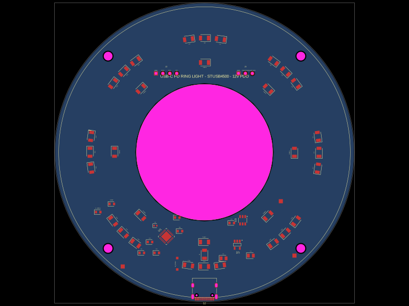 More from this authorimrishabh18/ring-lightIt is a surface-mount voltage regulator integrated circuit (AP2112K-3.3) with pins for input, ground, enable, and output.
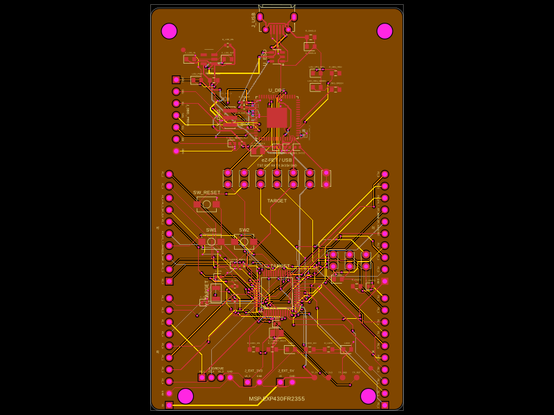 Similar packageShiboSoftwareDev/msp-exp430fr2355This code defines React components representing various surface-mount and through-hole electronic components—such as resonators, microcontrollers, crystals, connectors, and push buttons—with detailed physical footprints, 3D models, and pin configurations for PCB design.
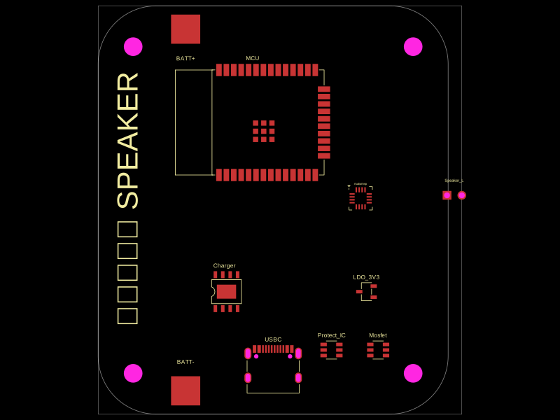 Discover something newmohan-bee/speakerThis code defines configurable 3D models and PCB footprints for various electronic components, including a battery charger IC, a dual Hall sensor, a dual power switch, and a voltage regulator, with detailed pinouts, footprints, and CAD models for schematic and physical design.