imrishabh18/corne-keyboard
The code defines and renders two surface-mount chip components with SMT pads, silkscreen outlines, and 3D CAD models (OBJ and STEP) for PCB assembly.
- Version
- 2.0.21
- License
- unset
- Stars
- 1
imports/PJ_399B_6A/PJ_399B_6A.tsx
import objPath from "./PJ_399B_6A.obj"
import stepPath from "./PJ_399B_6A.step"
import type { ChipProps } from "@tscircuit/props"

const pinLabels = {
  pin1: ["pin1"],
  pin2: ["pin2"],
  pin3: ["pin3"],
  pin4: ["pin4"],
  pin5: ["pin5"],
  pin6: ["pin6"]
} as const

export const PJ_399B_6A = (props: ChipProps<typeof pinLabels>) => {
  return (
    <chip
      pinLabels={pinLabels}
      symbol={
        <symbol>
          <port name="pin1" pinNumber={1} aliases={["1"]} direction="right" schX={6.35} schY={5.08} schStemLength={5.08} />
          <port name="pin2" pinNumber={2} aliases={["2"]} direction="right" schX={6.35} schY={2.54} schStemLength={5.08} />
          <port name="pin3" pinNumber={3} aliases={["3"]} direction="right" schX={6.35} schY={0} schStemLength={5.08} />
          <port name="pin4" pinNumber={4} aliases={["4"]} direction="right" schX={6.35} schY={-7.62} schStemLength={5.08} />
          <port name="pin5" pinNumber={5} aliases={["5"]} direction="right" schX={6.35} schY={-2.54} schStemLength={5.08} />
          <port name="pin6" pinNumber={6} aliases={["6"]} direction="right" schX={6.35} schY={-5.08} schStemLength={5.08} />
          <schematicpath points={[{"x":1.27,"y":5.08},{"x":-8.128,"y":5.08},{"x":-8.128,"y":0.762},{"x":-8.636,"y":1.778},{"x":-8.636,"y":1.778}]} strokeWidth={0.254} strokeColor="#880000" />
          <schematicpath points={[{"x":1.27,"y":-7.62},{"x":-8.128,"y":-7.62},{"x":-8.128,"y":-3.302},{"x":-8.636,"y":-4.318},{"x":-8.636,"y":-4.318}]} strokeWidth={0.254} strokeColor="#880000" />
          <schematicpath points={[{"x":1.27,"y":2.54},{"x":-4.826,"y":2.54},{"x":-5.334,"y":1.27},{"x":-5.842,"y":2.54}]} strokeWidth={0.254} strokeColor="#880000" />
          <schematicpath points={[{"x":1.27,"y":0},{"x":-3.81,"y":0},{"x":-4.318,"y":-0.762},{"x":-4.826,"y":0}]} strokeWidth={0.254} strokeColor="#880000" />
          <schematicpath points={[{"x":1.27,"y":-5.08},{"x":-4.826,"y":-5.08},{"x":-5.334,"y":-3.81},{"x":-5.842,"y":-5.08}]} strokeWidth={0.254} strokeColor="#880000" />
          <schematicpath points={[{"x":1.27,"y":-2.54},{"x":-3.81,"y":-2.54},{"x":-4.318,"y":-1.778},{"x":-4.826,"y":-2.54}]} strokeWidth={0.254} strokeColor="#880000" />
        </symbol>
      }
      supplierPartNumbers={{
  "jlcpcb": [
    "C128994"
  ]
}}
      manufacturerPartNumber="PJ_399B_6A"
      footprint={<footprint>
        <platedhole  portHints={["pin1"]} pcbX="4.89990125mm" pcbY="3.850005mm" holeWidth="1.4999462mm" holeHeight="0.599948mm" outerWidth="2.1999956mm" outerHeight="1.2999974mm" shape="pill" />
<platedhole  portHints={["pin2"]} pcbX="1.70000925mm" pcbY="3.850767mm" holeWidth="1.4999462mm" holeHeight="0.599948mm" outerWidth="2.1999956mm" outerHeight="1.2999974mm" shape="pill" />
<platedhole  portHints={["pin4"]} pcbX="4.80592125mm" pcbY="-3.809873mm" holeWidth="1.4999462mm" holeHeight="0.599948mm" outerWidth="2.1999956mm" outerHeight="1.2999974mm" shape="pill" />
<platedhole  portHints={["pin6"]} pcbX="1.70000925mm" pcbY="-3.850513mm" holeWidth="1.4999462mm" holeHeight="0.599948mm" outerWidth="2.1999956mm" outerHeight="1.2999974mm" shape="pill" />
<smtpad portHints={["pin3"]} pcbX="-4.19990275mm" pcbY="3.799967mm" width="1.499997mm" height="1.400048mm" shape="rect" />
<smtpad portHints={["pin5"]} pcbX="-4.19990275mm" pcbY="-3.799967mm" width="1.499997mm" height="1.400048mm" shape="rect" />
<silkscreenpath route={[{"x":-0.2740787500000579,"y":-3.0478729999999814},{"x":-0.2740787500000579,"y":-4.063872999999944},{"x":-2.052078749999964,"y":-4.063872999999944},{"x":-2.052078749999964,"y":-3.0478729999999814}]} />
<silkscreenpath route={[{"x":7.5999212500000795,"y":3.0001210000000356},{"x":-5.0000027500000215,"y":3.0001210000000356}]} />
<silkscreenpath route={[{"x":7.5999212500000795,"y":-2.9998669999999947},{"x":-5.0000027500000215,"y":-2.9998669999999947}]} />
<silkscreenpath route={[{"x":-5.0000027500000215,"y":3.0001210000000356},{"x":-5.0000027500000215,"y":-2.9998669999999947}]} />
<silkscreenpath route={[{"x":7.600937250000015,"y":3.0001210000000356},{"x":7.600937250000015,"y":-2.9998669999999947}]} />
<silkscreenpath route={[{"x":7.5999212500000795,"y":2.540126999999984},{"x":10.139921250000043,"y":2.540126999999984},{"x":10.139921250000043,"y":-2.539872999999943},{"x":7.5999212500000795,"y":-2.539872999999943}]} />
<silkscreenpath route={[{"x":-2.052078749999964,"y":3.0481270000000222},{"x":-2.052078749999964,"y":4.064127000000099},{"x":-0.2740787500000579,"y":4.064127000000099},{"x":-0.2740787500000579,"y":3.0481270000000222}]} />
<silkscreentext text="{NAME}" pcbX="2.57072125mm" pcbY="5.495927mm" anchorAlignment="center" fontSize="1mm" />
<fabricationnotepath route={[{"x":7.549984849999987,"y":2.5001220000001467},{"x":10.049979850000113,"y":2.5001220000001467},{"x":10.049979850000113,"y":-2.499867999999992},{"x":7.549984849999987,"y":-2.499867999999992},{"x":7.549984849999987,"y":2.5001220000001467}]} strokeWidth="0.254mm" />
<courtyardoutline outline={[{"x":-5.248478750000004,"y":4.745926999999938},{"x":10.389921250000043,"y":4.745926999999938},{"x":10.389921250000043,"y":-4.745673000000011},{"x":-5.248478750000004,"y":-4.745673000000011},{"x":-5.248478750000004,"y":4.745926999999938}]} />
      </footprint>}
      cadModel={{
        objUrl: objPath,
        stepUrl: stepPath,
        pcbRotationOffset: 0,
        modelOriginPosition: { x: -2.4329892499999914, y: -0.00013970000009067007, z: -0.10000480000000023 },
      }}
      {...props}
    />
  )
}
Related Packages
 More from this authorimrishabh18/boost-converterThis code defines a PCB schematic and 3D model layout focusing on a power conversion circuit with components like USB-C connector, MT3608 step-up regulator, inductor, diode, input/output capacitors, and resistors arranged on a double-layer PCB.
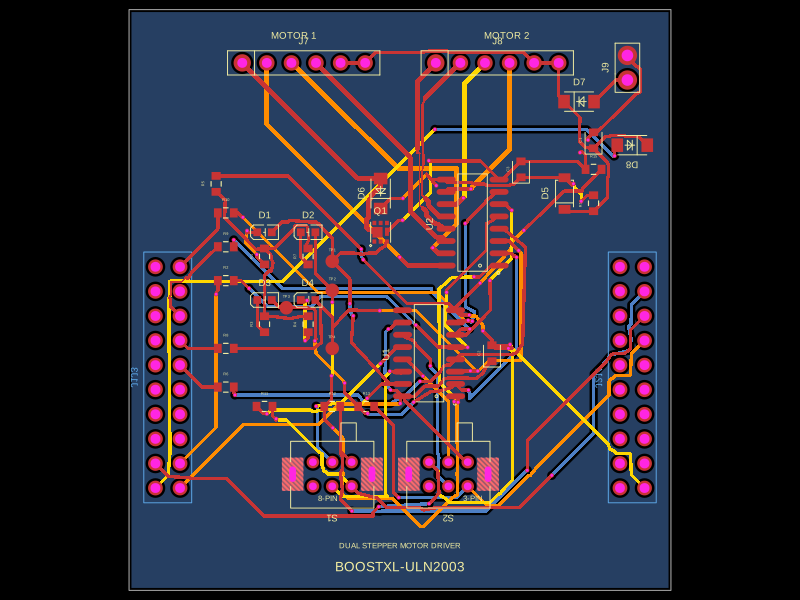 Similar packageabse/boostxl-uln2003This code defines a React component that models a through-hole or surface-mount LED with specified pin labels, footprint, silkscreen, and 3D CAD model for PCB layout.
 Discover something newhrithik18k/smart-switch-pcbThe AO3400A component models a SOT-23 N-channel MOSFET with labeled pins for Gate, Source, and Drain, including 3D CAD models and schematic symbols for electronic circuit design.