huntiep/radio
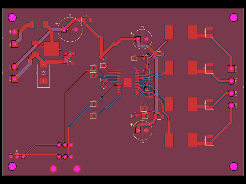
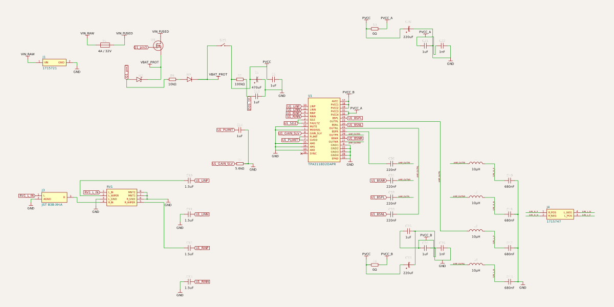
A 12‑V car-powered stereo aux amplifier PCB using a TPA3118D2 class‑D BTL amp, protected power input, dual-gang volume control, LC speaker filters, and four-wire left/right speaker outputs.
- Version
- 0.0.1
- License
- unset
- Stars
- 0
index.tsx
PCB
Schematic
/**
 * Car "radio" — aux-in stereo amplifier
 * ------------------------------------------------------------
 * 12 V car power -> fuse -> reverse-polarity P-FET -> TVS clamp
 *   -> panel power switch -> TPA3118D2 2x class-D amp (BTL, 20 dB)
 *   -> 10 uH / 680 nF LC filters -> 4 Ω speakers
 * Aux in (3.5 mm panel jack via header) -> dual-gang 10 kΩ log pot
 *   -> AC coupling -> amp inputs
 *
 * Board: 100 x 70 mm, 2 layers, GND pours on both layers.
 * PCB origin is the board centre, +Y is up.
 */

/* ---------------------------------------------------------------
 * Custom footprints (dimensions from typical datasheets — check
 * each one against the exact part you buy before ordering boards)
 * ------------------------------------------------------------- */

// Littelfuse 451/453 "Nano2" 2410 SMD fuse, e.g. 0451004.MRL (4 A)
const Fuse2410 = (
  <footprint>
    <smtpad portHints={["pin1"]} shape="rect" pcbX={-2.8} pcbY={0} width={2.0} height={3.0} />
    <smtpad portHints={["pin2"]} shape="rect" pcbX={2.8} pcbY={0} width={2.0} height={3.0} />
  </footprint>
)

// 12 x 12 mm shielded power inductor (e.g. Würth WE-PD 1260 / Bourns SRP1265A)
const Inductor1212 = (
  <footprint>
    <smtpad portHints={["pin1"]} shape="rect" pcbX={-4.9} pcbY={0} width={3.6} height={5.6} />
    <smtpad portHints={["pin2"]} shape="rect" pcbX={4.9} pcbY={0} width={3.6} height={5.6} />
  </footprint>
)

// 9 mm dual-gang rotary pot, PCB mount (Alps RK09-style), shaft facing board edge.
// Front row = gang A (pins 1-3), back row = gang B (pins 4-6), plus 2 mounting legs.
const DualPot9mm = (
  <footprint>
    <platedhole portHints={["pin1"]} shape="circle" pcbX={-2.5} pcbY={0} holeDiameter={1.0} outerDiameter={1.8} />
    <platedhole portHints={["pin2"]} shape="circle" pcbX={0} pcbY={0} holeDiameter={1.0} outerDiameter={1.8} />
    <platedhole portHints={["pin3"]} shape="circle" pcbX={2.5} pcbY={0} holeDiameter={1.0} outerDiameter={1.8} />
    <platedhole portHints={["pin4"]} shape="circle" pcbX={-2.5} pcbY={5} holeDiameter={1.0} outerDiameter={1.8} />
    <platedhole portHints={["pin5"]} shape="circle" pcbX={0} pcbY={5} holeDiameter={1.0} outerDiameter={1.8} />
    <platedhole portHints={["pin6"]} shape="circle" pcbX={2.5} pcbY={5} holeDiameter={1.0} outerDiameter={1.8} />
    <platedhole portHints={["pin7"]} shape="circle" pcbX={-4.9} pcbY={-5} holeDiameter={2.2} outerDiameter={3.2} />
    <platedhole portHints={["pin8"]} shape="circle" pcbX={4.9} pcbY={-5} holeDiameter={2.2} outerDiameter={3.2} />
  </footprint>
)

// TI DAP0032C (HTSSOP-32, PowerPAD down) per the datasheet land pattern:
// 0.65 mm pitch, 1.5 x 0.45 mm pads on a 7.5 mm row-to-row centre line,
// 3.04 x 3.74 mm exposed pad (pin 33) with 12 x 0.3 mm thermal vias to the bottom pour.
const pinY = (i: number) => 4.875 - 0.65 * i
const thermalVias: [number, number][] = []
for (const x of [-1, 0, 1]) for (const y of [-1.5, -0.5, 0.5, 1.5]) thermalVias.push([x, y])
const HTSSOP32_DAP = (
  <footprint>
    {Array.from({ length: 16 }, (_, i) => (
      <smtpad key={`l${i}`} portHints={[`pin${i + 1}`]} shape="rect" pcbX={-3.75} pcbY={pinY(i)} width={1.5} height={0.45} />
    ))}
    {Array.from({ length: 16 }, (_, i) => (
      <smtpad key={`r${i}`} portHints={[`pin${32 - i}`]} shape="rect" pcbX={3.75} pcbY={pinY(i)} width={1.5} height={0.45} />
    ))}
    <smtpad portHints={["pin33"]} shape="rect" pcbX={0} pcbY={0} width={3.04} height={3.74} />
    {thermalVias.map(([x, y], i) => (
      <platedhole key={`v${i}`} portHints={["pin33"]} shape="circle" pcbX={x} pcbY={y} holeDiameter={0.3} outerDiameter={0.6} />
    ))}
  </footprint>
)

// DPAK (TO-252): pin 1 = gate, pin 3 = source, tab = drain
const DPAK_PFET = (
  <footprint>
    <smtpad portHints={["pin3"]} shape="rect" pcbX={-3.42} pcbY={2.29} width={3.0} height={1.6} />
    <smtpad portHints={["pin2"]} shape="rect" pcbX={-3.42} pcbY={-2.29} width={3.0} height={1.6} />
    <smtpad portHints={["pin1"]} shape="rect" pcbX={3.42} pcbY={0} width={6.2} height={5.8} />
  </footprint>
)

const AMP_X = 2
const AMP_Y = 4

export default () => (
  <board width="100mm" height="70mm" layers={2} minTraceWidth="0.25mm" autorouterEffortLevel="5x">
    {/* Net classes: wide copper for the high-current paths */}
    <net name="GND" isGroundNet />
    <net name="VIN_RAW" isPowerNet nominalTraceWidth="1.5mm" />
    <net name="VIN_FUSED" isPowerNet nominalTraceWidth="1.5mm" />
    <net name="VBAT_PROT" isPowerNet nominalTraceWidth="1.5mm" />
    <net name="PVCC" isPowerNet nominalTraceWidth="1.2mm" />
    <net name="PVCC_A" isPowerNet nominalTraceWidth="0.45mm" />
    <net name="PVCC_B" isPowerNet nominalTraceWidth="0.45mm" />
    <net name="AMP_OUTPR" nominalTraceWidth="0.6mm" />
    <net name="AMP_OUTNR" nominalTraceWidth="0.6mm" />
    <net name="AMP_OUTPL" nominalTraceWidth="0.6mm" />
    <net name="AMP_OUTNL" nominalTraceWidth="0.6mm" />
    <net name="SPK_R_P" nominalTraceWidth="1mm" />
    <net name="SPK_R_N" nominalTraceWidth="1mm" />
    <net name="SPK_L_P" nominalTraceWidth="1mm" />
    <net name="SPK_L_N" nominalTraceWidth="1mm" />

    {/* ======================= POWER INPUT ======================= */}
    {/* J1: 12 V in — pin1 = +12 V (switched ACC or fused battery), pin2 = GND/chassis */}
    <connector
      name="J1"
      manufacturerPartNumber="1715721"
      footprint="pinrow2_p5.08mm_id1.3mm_od2.6mm"
      pinLabels={{ pin1: "VIN", pin2: "GND" }}
      pcbX={-45}
      pcbY={22.5}
      pcbRotation={90}
      schX={-16}
      schY={4}
    />

    {/* F1: 4 A fast fuse */}
    <fuse name="F1" manufacturerPartNumber="0451004.MRL" currentRating="4A" voltageRating="32V" footprint={Fuse2410} pcbX={-35} pcbY={28} schX={-13} schY={5} />

    {/* Q1: P-MOSFET reverse-battery protection (ideal diode).
        Drain to fuse, source to protected rail, gate pulled to GND.
        e.g. Infineon IPD50P04P4L-11 (-40 V, AEC-Q101) */}
    <mosfet
      name="Q1"
      channelType="p"
      mosfetMode="enhancement"
      footprint={DPAK_PFET}
      manufacturerPartNumber="IPD50P04P4L-11"
      pcbX={-33}
      pcbY={18}
      schX={-10}
      schY={5}
    />
    {/* Gate pull-down and 12 V zener gate clamp (protects Vgs during spikes) */}
    <resistor name="R1" resistance="10k" footprint="0805" pcbX={-22} pcbY={12} schX={-9} schY={3} />
    <diode name="D2" zener manufacturerPartNumber="MMSZ5242B" footprint="sod123" pcbX={-22} pcbY={16} schX={-11} schY={3} />

    {/* D1: TVS — clamps load-dump / inductive spikes below the amp's 30 V abs max */}
    <diode name="D1" tvs manufacturerPartNumber="SMCJ18A" footprint="smc" pcbX={-33} pcbY={8} pcbRotation={90} schX={-8} schY={3} />

    {/* J2: panel-mount power switch (SPST, >= 5 A) wired to this terminal */}
    <switch
      name="SW1"
      spst
      footprint="pinrow2_p5.08mm_id1.3mm_od2.6mm"
      pcbX={-45}
      pcbY={8}
      pcbRotation={90}
      schX={-6}
      schY={5}
    />

    {/* Bulk reservoir after the switch */}
    <capacitor name="C1" capacitance="470uF" polarized maxVoltageRating="35V" footprint="electrolytic_d10mm_p5mm" pcbX={-22} pcbY={26} schX={-4} schY={3} />
    <capacitor name="C2" capacitance="1uF" maxVoltageRating="50V" footprint="1206" pcbX={-15} pcbY={30} schX={-3} schY={3} />

    <trace from=".J1 > .VIN" to="net.VIN_RAW" />
    <trace from=".F1 > .pin1" to="net.VIN_RAW" />
    <trace from=".F1 > .pin2" to="net.VIN_FUSED" />
    <trace from=".Q1 > .drain" to="net.VIN_FUSED" />
    <trace from=".Q1 > .source" to="net.VBAT_PROT" />
    <trace from=".Q1 > .gate" to=".R1 > .pin1" />
    <trace from=".R1 > .pin2" to="net.GND" />
    <trace from=".D2 > .cathode" to="net.VBAT_PROT" />
    <trace from=".D2 > .anode" to=".Q1 > .gate" />
    <trace from=".D1 > .cathode" to="net.VBAT_PROT" />
    <trace from=".D1 > .anode" to="net.GND" />
    <trace from=".SW1 > .pin1" to="net.VBAT_PROT" />
    <trace from=".SW1 > .pin2" to="net.PVCC" />
    <trace from=".C1 > .pos" to="net.PVCC" />
    <trace from=".C1 > .neg" to="net.GND" />
    <trace from=".C2 > .pin1" to="net.PVCC" />
    <trace from=".C2 > .pin2" to="net.GND" />
    <trace from=".J1 > .GND" to="net.GND" />

    {/* ======================= AUDIO INPUT ======================= */}
    {/* J3: to 3.5 mm panel jack (JST-XH 3-pin). Use shielded cable. */}
    <connector
      name="J3"
      manufacturerPartNumber="JST B3B-XH-A"
      footprint="pinrow3_p2.5mm"
      pinLabels={{ pin1: "L", pin2: "AGND", pin3: "R" }}
      pcbX={-44}
      pcbY={-27}
      schX={-16}
      schY={-4}
    />

    {/* RV1: dual-gang 10 kΩ log (A) volume pot.
        Gang A = left (pins 1-3), gang B = right (pins 4-6).
        Pin 1/4 = signal in (CW end), 2/5 = wiper, 3/6 = ground (CCW end). */}
    <chip
      name="RV1"
      footprint={DualPot9mm}
      pinLabels={{
        pin1: "L_IN",
        pin2: "L_WIPER",
        pin3: "L_GND",
        pin4: "R_IN",
        pin5: "R_WIPER",
        pin6: "R_GND",
        pin7: "MNT1",
        pin8: "MNT2",
      }}
      pcbX={-24}
      pcbY={-27}
      schX={-12}
      schY={-4}
    />
    <trace from=".J3 > .L" to=".RV1 > .L_IN" />
    <trace from=".J3 > .R" to=".RV1 > .R_IN" />
    <trace from=".J3 > .AGND" to="net.GND" />
    <trace from=".RV1 > .L_GND" to="net.GND" />
    <trace from=".RV1 > .R_GND" to="net.GND" />
    <trace from=".RV1 > .MNT1" to="net.GND" />
    <trace from=".RV1 > .MNT2" to="net.GND" />

    {/* Input AC coupling: 1.5 uF (TI-recommended for 20 dB / 60 kΩ input).
        Negative inputs are AC-grounded with matching caps. */}
    <capacitor name="C10" capacitance="1.5uF" maxVoltageRating="25V" footprint="0805" pcbX={-12} pcbY={-5} schX={-8} schY={-3} />
    <capacitor name="C11" capacitance="1.5uF" maxVoltageRating="25V" footprint="0805" pcbX={-12} pcbY={-10} schX={-8} schY={-5} />
    <capacitor name="C12" capacitance="1.5uF" maxVoltageRating="25V" footprint="0805" pcbX={-12} pcbY={10} schX={-8} schY={-7} />
    <capacitor name="C13" capacitance="1.5uF" maxVoltageRating="25V" footprint="0805" pcbX={-12} pcbY={7} schX={-8} schY={-9} />
    <trace from=".RV1 > .L_WIPER" to=".C10 > .pin1" />
    <trace from=".C10 > .pin2" to=".U1 > .LINP" />
    <trace from=".C11 > .pin1" to="net.GND" />
    <trace from=".C11 > .pin2" to=".U1 > .LINN" />
    <trace from=".RV1 > .R_WIPER" to=".C12 > .pin1" />
    <trace from=".C12 > .pin2" to=".U1 > .RINP" />
    <trace from=".C13 > .pin1" to="net.GND" />
    <trace from=".C13 > .pin2" to=".U1 > .RINN" />

    {/* ======================= AMPLIFIER ======================= */}
    {/* U1: TPA3118D2DAP — HTSSOP-32, PowerPAD DOWN (soldered to board).
        (TPA3116D2 is pin-compatible but its DAD package has the pad on top
        and needs a clip-on heatsink — it will NOT use this thermal pad.) */}
    <chip
      name="U1"
      manufacturerPartNumber="TPA3118D2DAPR"
      footprint={HTSSOP32_DAP}
      pinLabels={{
        pin1: "MODSEL",
        pin2: "SDZ",
        pin3: "FAULTZ",
        pin4: "RINP",
        pin5: "RINN",
        pin6: "PLIMIT",
        pin7: "GVDD",
        pin8: "GAIN_SLV",
        pin9: "GND1",
        pin10: "LINP",
        pin11: "LINN",
        pin12: "MUTE",
        pin13: "AM2",
        pin14: "AM1",
        pin15: "AM0",
        pin16: "SYNC",
        pin17: "AVCC",
        pin18: "PVCC1",
        pin19: "PVCC2",
        pin20: "BSNL",
        pin21: "OUTNL",
        pin22: "GND2",
        pin23: "OUTPL",
        pin24: "BSPL",
        pin25: "GND3",
        pin26: "BSNR",
        pin27: "OUTNR",
        pin28: "GND4",
        pin29: "OUTPR",
        pin30: "BSPR",
        pin31: "PVCC3",
        pin32: "PVCC4",
        pin33: "EPAD",
      }}
      schPinArrangement={{
        leftSide: {
          direction: "top-to-bottom",
          pins: ["LINP", "LINN", "RINP", "RINN", "SDZ", "FAULTZ", "MUTE", "MODSEL", "GAIN_SLV", "PLIMIT", "GVDD", "AM0", "AM1", "AM2", "SYNC"],
        },
        rightSide: {
          direction: "top-to-bottom",
          pins: ["AVCC", "PVCC1", "PVCC2", "PVCC3", "PVCC4", "BSPL", "OUTPL", "BSNL", "OUTNL", "BSPR", "OUTPR", "BSNR", "OUTNR", "GND1", "GND2", "GND3", "GND4", "EPAD"],
        },
      }}
      noConnect={["SYNC"]}
      pcbX={AMP_X}
      pcbY={AMP_Y}
      schX={0}
      schY={0}
    />

    {/* Supply pins */}
    <trace from=".U1 > .PVCC1" to="net.PVCC_B" />
    <trace from=".U1 > .PVCC2" to="net.PVCC_B" />
    <trace from=".U1 > .PVCC3" to="net.PVCC_A" />
    <trace from=".U1 > .PVCC4" to="net.PVCC_A" />
    <trace from=".U1 > .AVCC" to="net.PVCC_B" />
    <trace from=".U1 > .GND1" to="net.GND" />
    <trace from=".U1 > .GND2" to="net.GND" />
    <trace from=".U1 > .GND3" to="net.GND" />
    <trace from=".U1 > .GND4" to="net.GND" />
    <trace from=".U1 > .EPAD" to="net.GND" />

    {/* Mode straps: BD modulation, 400 kHz, master, unmuted, no power limit */}
    <trace from=".U1 > .MODSEL" to="net.GND" />
    <trace from=".U1 > .MUTE" to="net.GND" />
    <trace from=".U1 > .AM0" to="net.GND" />
    <trace from=".U1 > .AM1" to="net.GND" />
    <trace from=".U1 > .AM2" to="net.GND" />
    <trace from=".U1 > .PLIMIT" to=".U1 > .GVDD" />

    {/* Gain = 20 dB master: 5.6 kΩ GAIN/SLV to GND, nothing to GVDD */}
    <resistor name="R2" resistance="5.6k" footprint="0603" pcbX={-8} pcbY={2} schX={-5} schY={-2} />
    <trace from=".R2 > .pin1" to=".U1 > .GAIN_SLV" />
    <trace from=".R2 > .pin2" to="net.GND" />

    {/* GVDD decoupling — nothing else may load this pin */}
    <capacitor name="C14" capacitance="1uF" maxVoltageRating="16V" footprint="0603" pcbX={-8} pcbY={5} schX={-5} schY={0} />
    <trace from=".C14 > .pin1" to=".U1 > .GVDD" />
    <trace from=".C14 > .pin2" to="net.GND" />

    {/* AVCC decoupling */}
    <capacitor name="C15" capacitance="1uF" maxVoltageRating="50V" footprint="0805" pcbX={9} pcbY={-7} schX={5} schY={-6} />
    <trace from=".C15 > .pin1" to="net.PVCC_B" />
    <trace from=".C15 > .pin2" to="net.GND" />

    {/* SDZ soft-start: 100 kΩ from PVCC (also the slew-rate resistor the
        datasheet asks for) + 1 uF delays un-mute ~100 ms so the input caps settle.
        FAULTZ (open drain) tied to SDZ = automatic recovery after a fault. */}
    <resistor name="R3" resistance="100k" footprint="0603" pcbX={-8} pcbY={14} schX={-5} schY={3} />
    <capacitor name="C16" capacitance="1uF" maxVoltageRating="25V" footprint="0603" pcbX={-8} pcbY={11} schX={-4} schY={2} />
    <trace from=".R3 > .pin1" to="net.PVCC" />
    <trace from=".R3 > .pin2" to=".U1 > .SDZ" />
    <trace from=".C16 > .pin1" to=".U1 > .SDZ" />
    <trace from=".C16 > .pin2" to="net.GND" />
    <trace from=".U1 > .FAULTZ" to=".U1 > .SDZ" />

    {/* PVCC decoupling at each end of the chip: bulk + 1 uF + 1 nF */}
    <capacitor name="C20" capacitance="220uF" polarized maxVoltageRating="35V" footprint="electrolytic_d8mm_p3.5mm" pcbX={8} pcbY={22} schX={5} schY={6} />
    <capacitor name="C21" capacitance="1uF" maxVoltageRating="50V" footprint="0805" pcbX={9.5} pcbY={14} schX={6} schY={5} />
    <capacitor name="C22" capacitance="1nF" maxVoltageRating="50V" footprint="0603" pcbX={5} pcbY={14} schX={7} schY={5} />
    <capacitor name="C23" capacitance="220uF" polarized maxVoltageRating="35V" footprint="electrolytic_d8mm_p3.5mm" pcbX={8} pcbY={-16} schX={5} schY={-8} />
    <capacitor name="C24" capacitance="1uF" maxVoltageRating="50V" footprint="0805" pcbX={9.5} pcbY={-10} schX={6} schY={-7} />
    <capacitor name="C25" capacitance="1nF" maxVoltageRating="50V" footprint="0603" pcbX={5} pcbY={-10} schX={7} schY={-7} />
    {["C21", "C22", "C24", "C25"].flatMap((c) => [
      <trace key={`${c}a`} from={`.${c} > .pin1`} to={c < "C23" ? "net.PVCC_A" : "net.PVCC_B"} />,
      <trace key={`${c}b`} from={`.${c} > .pin2`} to="net.GND" />,
    ])}
    <trace from=".C20 > .pos" to="net.PVCC" />
    <trace from=".C20 > .neg" to="net.GND" />
    <trace from=".C23 > .pos" to="net.PVCC" />
    <trace from=".C23 > .neg" to="net.GND" />


    {/* 0 Ω links (1206, >= 2 A) join the wide PVCC bus to each pair of narrow
        chip PVCC pins. They are just copper; they let the bus stay 1.2 mm wide
        right up to the IC while the pin fan-out stays fine-pitch. */}
    <resistor name="R4" resistance="0" footprint="1206" pcbX={15} pcbY={16} schX={3} schY={6} />
    <resistor name="R5" resistance="0" footprint="1206" pcbX={15} pcbY={-10.5} schX={3} schY={-8} />
    <trace from=".R4 > .pin1" to="net.PVCC" />
    <trace from=".R4 > .pin2" to="net.PVCC_A" />
    <trace from=".R5 > .pin1" to="net.PVCC" />
    <trace from=".R5 > .pin2" to="net.PVCC_B" />

    {/* Bootstrap caps: 220 nF X7R >= 25 V, BSxx to its own output */}
    <capacitor name="C30" capacitance="220nF" maxVoltageRating="25V" footprint="0603" pcbX={10} pcbY={9} pcbRotation={90} schX={4} schY={-2} />
    <capacitor name="C31" capacitance="220nF" maxVoltageRating="25V" footprint="0603" pcbX={12} pcbY={6} pcbRotation={90} schX={4} schY={-3} />
    <capacitor name="C32" capacitance="220nF" maxVoltageRating="25V" footprint="0603" pcbX={10} pcbY={2} pcbRotation={90} schX={4} schY={-4} />
    <capacitor name="C33" capacitance="220nF" maxVoltageRating="25V" footprint="0603" pcbX={12} pcbY={-1} pcbRotation={90} schX={4} schY={-5} />
    <trace from=".C30 > .pin1" to=".U1 > .BSPR" />
    <trace from=".C30 > .pin2" to="net.AMP_OUTPR" />
    <trace from=".C31 > .pin1" to=".U1 > .BSNR" />
    <trace from=".C31 > .pin2" to="net.AMP_OUTNR" />
    <trace from=".C32 > .pin1" to=".U1 > .BSPL" />
    <trace from=".C32 > .pin2" to="net.AMP_OUTPL" />
    <trace from=".C33 > .pin1" to=".U1 > .BSNL" />
    <trace from=".C33 > .pin2" to="net.AMP_OUTNL" />

    {/* ======================= OUTPUT FILTER ======================= */}
    {/* 10 uH (Isat >= 6 A) + 680 nF per output, TI-recommended for 4 Ω BTL.
        Needed here because car speaker runs are long and the AM/FM radio
        antenna is nearby. */}
    <inductor name="L1" inductance="10uH" maxCurrentRating="6A" footprint={Inductor1212} manufacturerPartNumber="7447709100" pcbX={24} pcbY={25} schX={9} schY={-2} />
    <inductor name="L2" inductance="10uH" maxCurrentRating="6A" footprint={Inductor1212} manufacturerPartNumber="7447709100" pcbX={24} pcbY={10} schX={9} schY={-4} />
    <inductor name="L3" inductance="10uH" maxCurrentRating="6A" footprint={Inductor1212} manufacturerPartNumber="7447709100" pcbX={24} pcbY={-5} schX={9} schY={-6} />
    <inductor name="L4" inductance="10uH" maxCurrentRating="6A" footprint={Inductor1212} manufacturerPartNumber="7447709100" pcbX={24} pcbY={-20} schX={9} schY={-8} />
    <capacitor name="C40" capacitance="680nF" maxVoltageRating="50V" footprint="1210" pcbX={36} pcbY={25} pcbRotation={90} schX={11} schY={-3} />
    <capacitor name="C41" capacitance="680nF" maxVoltageRating="50V" footprint="1210" pcbX={36} pcbY={10} pcbRotation={90} schX={11} schY={-5} />
    <capacitor name="C42" capacitance="680nF" maxVoltageRating="50V" footprint="1210" pcbX={36} pcbY={-5} pcbRotation={90} schX={11} schY={-7} />
    <capacitor name="C43" capacitance="680nF" maxVoltageRating="50V" footprint="1210" pcbX={36} pcbY={-20} pcbRotation={90} schX={11} schY={-9} />

    <trace from=".U1 > .OUTPR" to="net.AMP_OUTPR" />
    <trace from=".L1 > .pin1" to="net.AMP_OUTPR" />
    <trace from=".U1 > .OUTNR" to="net.AMP_OUTNR" />
    <trace from=".L2 > .pin1" to="net.AMP_OUTNR" />
    <trace from=".U1 > .OUTPL" to="net.AMP_OUTPL" />
    <trace from=".L3 > .pin1" to="net.AMP_OUTPL" />
    <trace from=".U1 > .OUTNL" to="net.AMP_OUTNL" />
    <trace from=".L4 > .pin1" to="net.AMP_OUTNL" />
    <trace from=".L1 > .pin2" to="net.SPK_R_P" />
    <trace from=".L2 > .pin2" to="net.SPK_R_N" />
    <trace from=".L3 > .pin2" to="net.SPK_L_P" />
    <trace from=".L4 > .pin2" to="net.SPK_L_N" />
    <trace from=".C40 > .pin1" to="net.SPK_R_P" />
    <trace from=".C41 > .pin1" to="net.SPK_R_N" />
    <trace from=".C42 > .pin1" to="net.SPK_L_P" />
    <trace from=".C43 > .pin1" to="net.SPK_L_N" />
    <trace from=".C40 > .pin2" to="net.GND" />
    <trace from=".C41 > .pin2" to="net.GND" />
    <trace from=".C42 > .pin2" to="net.GND" />
    <trace from=".C43 > .pin2" to="net.GND" />

    {/* J4: speaker terminal. Never connect either speaker lead to chassis —
        both outputs are bridged (BTL) and swing around PVCC/2. */}
    <connector
      name="J4"
      manufacturerPartNumber="1715747"
      footprint="pinrow4_p5.08mm_id1.3mm_od2.6mm"
      pinLabels={{ pin1: "R_POS", pin2: "R_NEG", pin3: "L_POS", pin4: "L_NEG" }}
      pcbX={45}
      pcbY={2}
      pcbRotation={-90}
      schX={14}
      schY={-5}
    />
    <trace from=".J4 > .R_POS" to="net.SPK_R_P" />
    <trace from=".J4 > .R_NEG" to="net.SPK_R_N" />
    <trace from=".J4 > .L_POS" to="net.SPK_L_P" />
    <trace from=".J4 > .L_NEG" to="net.SPK_L_N" />

    {/* Ground pours on both layers */}
    <copperpour layer="top" connectsTo="net.GND" />
    <copperpour layer="bottom" connectsTo="net.GND" />

    {/* Mounting holes */}
    <hole diameter="3.2mm" pcbX={-46} pcbY={-31} />
    <hole diameter="3.2mm" pcbX={46} pcbY={-31} />
    <hole diameter="3.2mm" pcbX={-46} pcbY={31} />
    <hole diameter="3.2mm" pcbX={46} pcbY={31} />
  </board>
)
Related Packages
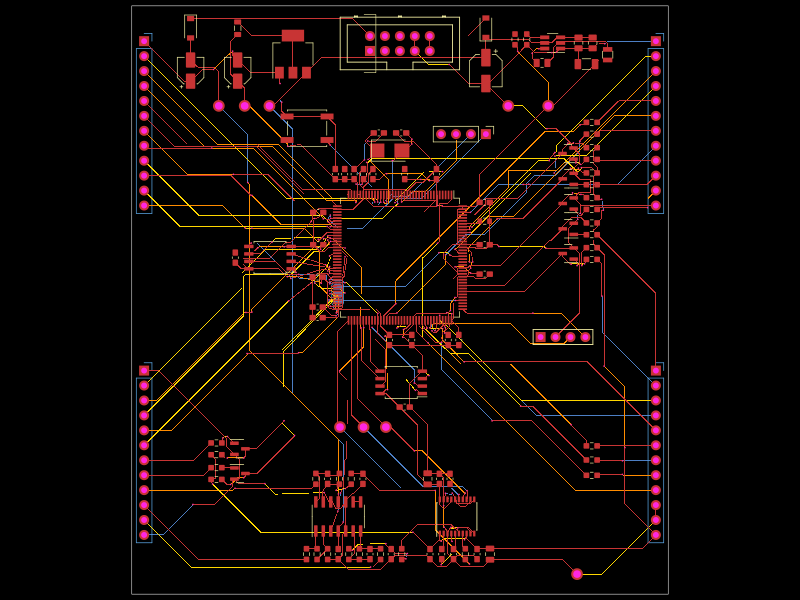 Similar packagehrithik18k/punck-tscircuit-recreationA four-layer Eurorack drum/sampler controller PCB built around an STM32H743, dual QSPI flash, PCM5100 stereo DAC, TL074 analog audio circuitry, input clamps, 12V-to-3.3V power regulation, MIDI/USB/SWD connectors, controls, LEDs, and trigger/audio I/O.
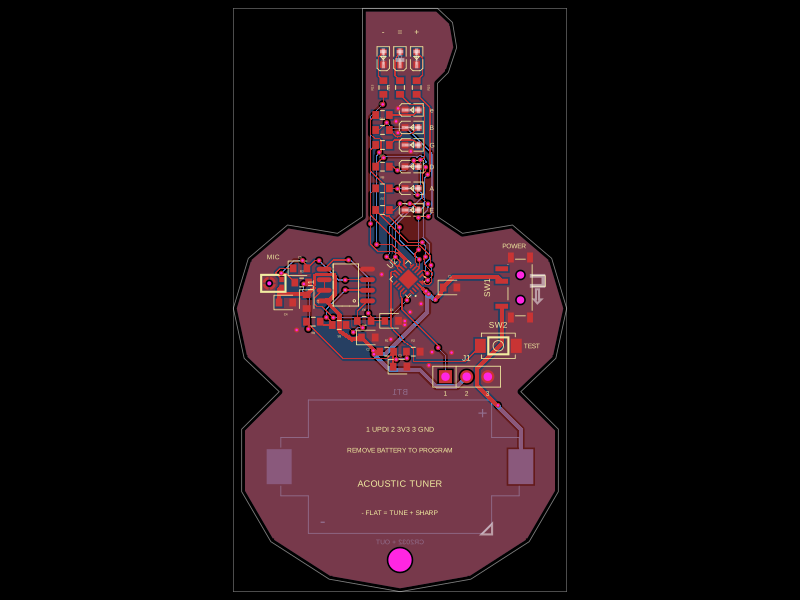 Discover something newgokul/acoustic-guitar-tunerThis code defines the physical pin configuration and footprint layouts for the ATtiny1616 microcontroller and a matching tactile switch component, including their key hardware connection points, dimensions, and 3D models.