hrithik18k/switch-pcb
A tscircuit package created by hrithik18k.
- Version
- 1.2.0
- License
- unset
- Stars
- 0
index.circuit.tsx
PCB

Schematic

import {A_0805W8F1002T5E} from "./imports/A_0805W8F1002T5E"
import {A_0805W8F1003T5E} from "./imports/A_0805W8F1003T5E"
import {A_2_54_1_3P_} from "./imports/A_2_54_1_3P_"
import {A_2_54_1_5P_} from "./imports/A_2_54_1_5P_"
import {CC0805KRX7R9BB104} from "./imports/CC0805KRX7R9BB104"
import {CL21A106KAYNNNE} from "./imports/CL21A106KAYNNNE"
import { ESP_12F_ESP8266MOD_ } from "./imports/ESP_12F_ESP8266MOD_"
import { AP2112K_3_3TRG1 } from "./imports/AP2112K_3_3TRG1"
export default () => <board width={50} height={48} layers={2} autorouter="auto-local" autorouterEffortLevel="5x" autorouterVersion="beta_pipeline1">
{["MCU","Power","Boot","Interfaces"].map(name=><schematicsection name={name} key={name}/>)}
<ESP_12F_ESP8266MOD_ name="U1" pcbX={-4} pcbY={5} pcbRotation={-90} schX={0} schY={0} schSectionName="MCU"/>
<keepout layers={["top","bottom"]} excludeRefs={[".U1"]} shape="rect" pcbX={-4} pcbY={19} width={28} height={10}/>
<AP2112K_3_3TRG1 name="U2" pcbX={-13} pcbY={-12} schX={-12} schY={0} schSectionName="Power"/>
<A_2_54_1_3P_ name="J1" pcbX={-14} pcbY={-20} schX={-18} schY={0} schSectionName="Power"/>
<CL21A106KAYNNNE name="C1" pcbX={-18} pcbY={-13} schX={-16} schY={-3} schRotation={-90} schSectionName="Power"/>
<CL21A106KAYNNNE name="C2" pcbX={-8} pcbY={-12} schX={-4} schY={-3} schRotation={-90} schSectionName="Power"/>
<CC0805KRX7R9BB104 name="C3" pcbX={-11} pcbY={-5} schX={-2.5} schY={-3} schRotation={-90} schSectionName="MCU"/>
<CL21A106KAYNNNE name="C4" pcbX={-6} pcbY={-5} schX={-1} schY={-3} schRotation={-90} schSectionName="MCU"/>
<A_0805W8F1002T5E name="R1" pcbX={-17} pcbY={8} schX={-4} schY={3} schRotation={90} schSectionName="Boot"/>
<A_0805W8F1002T5E name="R2" pcbX={-17} pcbY={12} schX={-2.5} schY={3} schRotation={90} schSectionName="Boot"/>
<A_0805W8F1002T5E name="R3" pcbX={11} pcbY={4} schX={-1} schY={3} schRotation={90} schSectionName="Boot"/>
<A_0805W8F1002T5E name="R4" pcbX={11} pcbY={0} schX={0.5} schY={3} schRotation={90} schSectionName="Boot"/>
<A_0805W8F1002T5E name="R5" pcbX={11} pcbY={-4} schX={-3} schY={0} schRotation={-90} schSectionName="Boot"/>
<A_0805W8F1003T5E name="R6" pcbX={14} pcbY={-11} schX={4} schY={0} schRotation={-90} schSectionName="Boot"/>
<A_2_54_1_5P_ name="J2" schWidth={0.58} pcbX={0} pcbY={-20} schX={0} schY={-6} schSectionName="Interfaces"/>
<A_2_54_1_3P_ name="J3" pcbX={19} pcbY={7} pcbRotation={90} schX={7} schY={-10} schSectionName="Interfaces"/>
<A_2_54_1_3P_ name="J4" pcbX={19} pcbY={-5} pcbRotation={90} schX={12} schY={-10} schSectionName="Interfaces"/>
<trace name="V5_0" from="J1.pin1" to="net.V5" width={0.25}/>
<trace name="V5_1" from="U2.VIN" to="net.V5" width={0.25}/>
<trace name="V5_2" from="U2.EN" to="net.V5" width={0.25}/>
<trace name="V5_3" from="C1.pin1" to="net.V5" width={0.25}/>
<trace name="V5_4" from="J3.pin1" to="net.V5" width={0.25}/>
<trace name="GND_0" from="J1.pin2" to="net.GND" width={0.25}/>
<trace name="GND_1" from="U2.GND" to="net.GND" width={0.25}/>
<trace name="GND_2" from="C1.pin2" to="net.GND" width={0.25}/>
<trace name="GND_3" from="C2.pin2" to="net.GND" width={0.25}/>
<trace name="GND_4" from="C3.pin2" to="net.GND" width={0.25}/>
<trace name="GND_5" from="C4.pin2" to="net.GND" width={0.25}/>
<trace name="GND_6" from="U1.GND" to="net.GND" width={0.25}/>
<trace name="GND_7" from="R5.pin2" to="net.GND" width={0.25}/>
<trace name="GND_8" from="R6.pin2" to="net.GND" width={0.25}/>
<trace name="GND_9" from="J2.pin1" to="net.GND" width={0.25}/>
<trace name="GND_10" from="J3.pin2" to="net.GND" width={0.25}/>
<trace name="GND_11" from="J4.pin2" to="net.GND" width={0.25}/>
<trace name="V3V3_0" from="U2.VOUT" to="net.V3V3" width={0.25}/>
<trace name="V3V3_1" from="U1.VCC" to="net.V3V3" width={0.25}/>
<trace name="V3V3_2" from="C2.pin1" to="net.V3V3" width={0.25}/>
<trace name="V3V3_3" from="C3.pin1" to="net.V3V3" width={0.25}/>
<trace name="V3V3_4" from="C4.pin1" to="net.V3V3" width={0.25}/>
<trace name="V3V3_5" from="R1.pin2" to="net.V3V3" width={0.25}/>
<trace name="V3V3_6" from="R2.pin2" to="net.V3V3" width={0.25}/>
<trace name="V3V3_7" from="R3.pin2" to="net.V3V3" width={0.25}/>
<trace name="V3V3_8" from="R4.pin2" to="net.V3V3" width={0.25}/>

<trace name="V3V3_10" from="J4.pin1" to="net.V3V3" width={0.25}/>
<trace name="EN_0" from="U1.EN" to="net.EN" width={0.15}/>
<trace name="EN_1" from="R1.pin1" to="net.EN" width={0.15}/>
<trace name="RST_0" from="U1.RST" to="net.RST" width={0.15}/>
<trace name="RST_1" from="R2.pin1" to="net.RST" width={0.15}/>
<trace name="RST_2" from="J2.pin5" to="net.RST" width={0.15}/>
<trace name="BOOT_0" from="U1.GPIO0" to="net.BOOT" width={0.15}/>
<trace name="BOOT_1" from="R3.pin1" to="net.BOOT" width={0.15}/>
<trace name="BOOT_2" from="J2.pin4" to="net.BOOT" width={0.15}/>
<trace name="STRAP2_0" from="U1.GPIO2" to="net.STRAP2" width={0.15}/>
<trace name="STRAP2_1" from="R4.pin1" to="net.STRAP2" width={0.15}/>
<trace name="STRAP15_0" from="U1.GPIO15" to="net.STRAP15" width={0.15}/>
<trace name="STRAP15_1" from="R5.pin1" to="net.STRAP15" width={0.15}/>
<trace name="RELAY_0" from="U1.GPIO12" to="net.RELAY" width={0.15}/>
<trace name="RELAY_1" from="J3.pin3" to="net.RELAY" width={0.15}/>
<trace name="RELAY_2" from="R6.pin1" to="net.RELAY" width={0.15}/>
<trace name="TOUCH_0" from="U1.GPIO13" to="net.TOUCH" width={0.15}/>
<trace name="TOUCH_1" from="J4.pin3" to="net.TOUCH" width={0.15}/>
<trace name="TXD_0" from="U1.TXD0" to="net.TXD" width={0.15}/>
<trace name="TXD_1" from="J2.pin2" to="net.TXD" width={0.15}/>
<trace name="RXD_0" from="U1.RXD0" to="net.RXD" width={0.15}/>
<trace name="RXD_1" from="J2.pin3" to="net.RXD" width={0.15}/>
{[-21,21].flatMap(x=>[-20,20].map(y=><hole key={x+","+y} pcbX={x} pcbY={y} diameter={3.2}/>))}
<silkscreentext text="SWITCH ESP12F REV B" pcbX={0} pcbY={-23} fontSize={0.9}/>
</board>
Related Packages
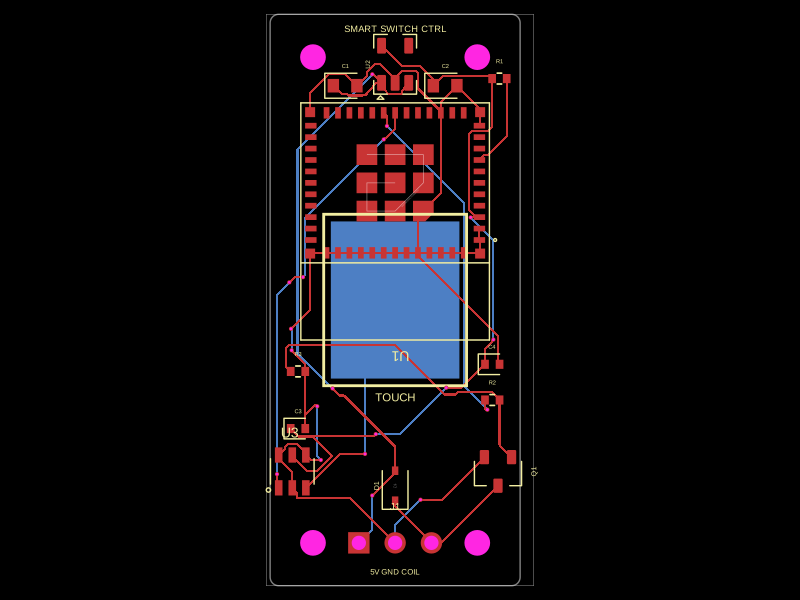 More from this authorhrithik18k/smart-switch-pcbThe AO3400A component models a SOT-23 N-channel MOSFET with labeled pins for Gate, Source, and Drain, including 3D CAD models and schematic symbols for electronic circuit design.
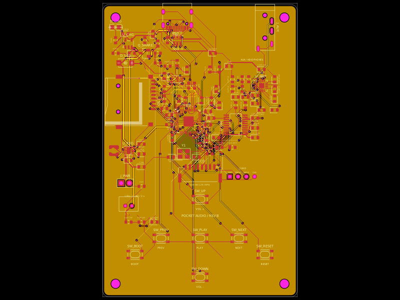 Discover something newDevesh36/pocket-audio-playerA portable, rechargeable microSD audio player built around an RP2040, SPI flash, USB‑C charging/power management, LCD/button controls, PCM5102A I²S DAC, and TPA6132A headphone amplifier in a 3D‑printed enclosure.