hrithik18k/smartknob-screen
A mixed SMT component library containing 3.3V regulators, resistors/capacitors, MOSFETs/transistors, USB-UART and sensor ICs, LEDs, connectors, an inductor, and related PCB footprints/CAD models.
- Version
- 1.0.3
- License
- Apache-2.0
- Stars
- 0
smartknob-board.tsx
import { importedParts } from './imported-parts'

/** Preserve the released KiCad land patterns. Supplier models supply MPN/BOM/3D data;
 * geometry and physical-pad aliases are deliberately overridden for exact placement.
 */
function ReferenceFootprint({ component: c }: { component: any }) {
  return <footprint insertionDirection={c.value.includes("USB") ? "from_y_neg" : "from_above"}>{c.pads.flatMap((p: any, i: number) => {
    const common = { pcbX: p.x, pcbY: p.y, portHints: [p.pin] }
    if (p.type === 'thru_hole') {
      if (p.drill[0] === 'oval') return <platedhole {...common} shape="pill" outerWidth={p.width} outerHeight={p.height} holeWidth={Number(p.drill[1])} holeHeight={Number(p.drill[2])} pcbRotation={p.rotation} />
      return <platedhole {...common} shape="circle" outerDiameter={p.width} holeDiameter={Number(p.drill[0])} />
    }
    if (p.shape === 'circle') return <smtpad {...common} layer={p.layer} shape="circle" radius={p.width / 2} coveredWithSolderMask={p.mask} />
    if (p.shape === 'oval') {
      return <smtpad {...common} layer={p.layer} shape="rotated_pill" width={p.width} height={p.height} radius={Math.min(p.width,p.height)/2} ccwRotation={p.rotation} coveredWithSolderMask={p.mask} />
    }
    if (p.shape === 'custom') return <smtpad {...common} layer={p.layer} shape="polygon" points={p.polygon} coveredWithSolderMask={p.mask} />
    return <smtpad {...common} layer={p.layer} shape="rotated_rect" width={p.width} height={p.height} ccwRotation={p.rotation} cornerRadius={p.radius ?? 0} coveredWithSolderMask={p.mask} />
  })}</footprint>
}

function Part({ component: c }: { component: any }) {
  const Component = c.importKey ? importedParts[c.importKey] : c.name === 'J2' && c.value.includes('USB') ? 'connector' : 'chip'
  const props: any = {
    name: c.name, ...(!c.importKey ? {manufacturerPartNumber: c.value} : {}),
    pcbX: c.x, pcbY: c.y, ...(c.layer === 'bottom' ? {layer: 'bottom'} : {}),
    schX: c.schX, schY: c.schY, schSectionName: c.section,

    schPinArrangement: {leftSide: {pins: Object.keys(c.pinLabels), direction: "top-to-bottom"}},
    pinLabels: c.pinLabels, pinAttributes: c.pinAttributes,
    shouldBeOnEdgeOfBoard: c.value.includes("USB"),
    allowOffBoard: c.value.includes("USB"),
    noConnect: c.noConnect, doNotPlace: c.doNotPlace,
    symbol: undefined, symbolName: undefined,
    footprint: <ReferenceFootprint component={c} />,
    pcbStyle: { silkscreenTextVisibility: 'hidden' },
    ...(c.lcsc ? {supplierPartNumbers: {jlcpcb: [c.lcsc]}} : {}),
    ...(c.name === 'NT1' ? {internallyConnectedPins: [['pin1', 'pin2']]} : {}),
  }
  return <Component {...props} />
}

/** Both boards have independent net scopes and should be built as separate entrypoints. */
export function SmartKnobBoard({ data }: { data: any }) {
  return <board width={Math.max(...data.outline.map((p: any) => p.x))-Math.min(...data.outline.map((p: any) => p.x))} height={Math.max(...data.outline.map((p: any) => p.y))-Math.min(...data.outline.map((p: any) => p.y))} title={data.title} outline={data.outline} thickness={data.thickness} layers={2} isViaInPadAllowed
    solderMaskColor="white" silkscreenColor="black" routingDisabled routeRemaining={false}
    // The checker boxes angled LED footprints axis-aligned and flags clear
    // flexure slots. Exact pad/body-to-cutout geometry is audited separately.
    placementDrcChecksDisabled={data.title.includes('Base')}
    pcbStyle={{silkscreenTextVisibility:'hidden'}}>
    {data.sections.map((name: string) => <schematicsection name={name} />)}
    {data.cutouts.map((points: any, i: number) => <cutout shape="polygon" points={points} />)}
    {data.holes.map((h: any, i: number) => <hole pcbX={h.x} pcbY={h.y} diameter={h.diameter} />)}
    {data.components.map((c: any) => <Part component={c} />)}
    {/* One source trace per net, in stable data.nets order. validate.py asserts
        that each explicit copper segment resolves to the expected source net. */}
    {data.nets.map((n: any) => <trace path={[...n.pins, `net.${n.name}`]} />)}
    {/* Core accepts the circuit-json source link; current JSX declarations omit it. */}
    {data.traces.map((t: any) => <pcbtrace {...({source_trace_id: `source_trace_${t.sourceIndex}`, route: t.route} as any)} />)}
    {data.vias.map((v: any, i: number) => <via pcbX={v.x} pcbY={v.y} holeDiameter={v.drill} outerDiameter={v.diameter} fromLayer="top" toLayer="bottom" connectsTo={`net.${v.net}`} />)}
    {data.pours.map((p: any, i: number) => <copperpour name={`POUR_${i}`} layer={p.layer} connectsTo={`net.${p.net}`} outline={p.outline} clearance={0} padMargin={0} traceMargin={0} boardEdgeMargin={0.22} cutoutMargin={0} />)}
  </board>
}
Related Packages
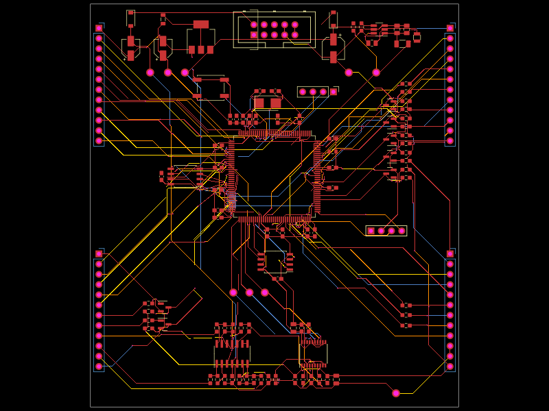 More from this authorhrithik18k/punck-tscircuit-recreationA four-layer Eurorack drum/sampler controller PCB built around an STM32H743, dual QSPI flash, PCM5100 stereo DAC, TL074 analog audio circuitry, input clamps, 12V-to-3.3V power regulation, MIDI/USB/SWD connectors, controls, LEDs, and trigger/audio I/O.
 Similar packagemohan-bee/esp32-c3This hardware design integrates an ESP32-C3 microcontroller, a USB-C connector, a power management IC (AP2112-3.3V regulator), a USB-to-Serial converter (CH340C), several resistors, capacitors, and user-accessible headers to facilitate USB communication, power regulation, and general I/O interfacing.
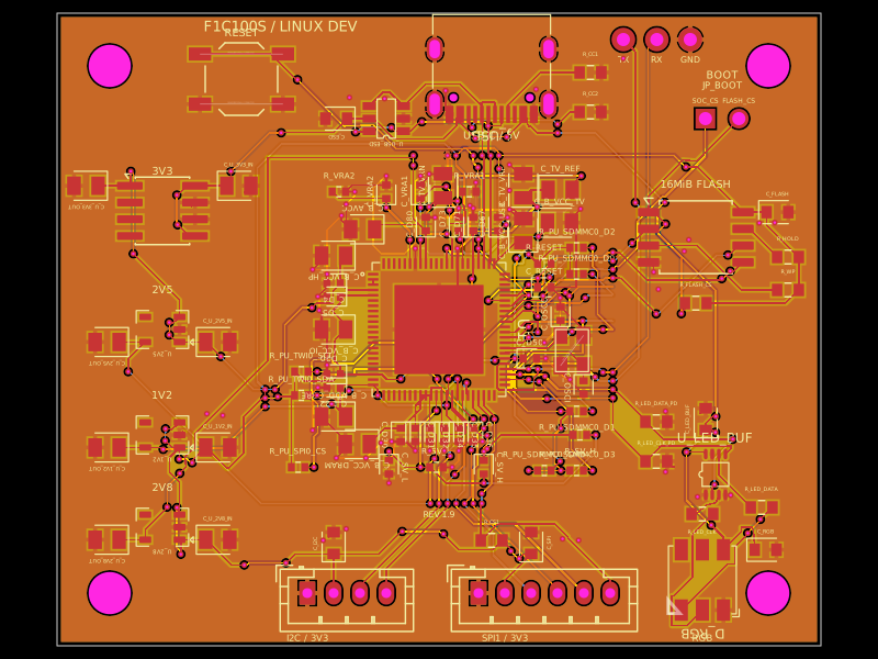 Discover something newseveibar/f1c100s-linux-dev-boardA 4-layer F1C100S Linux development carrier board with USB‑C power/data, multi-rail LDOs, SPI NOR flash, reset/boot interfaces, I²C/SPI/UART headers, ESD protection, and a buffered 5‑V clocked RGB LED.