hrithik18k/smart-switch-pcb
The AO3400A component models a SOT-23 N-channel MOSFET with labeled pins for Gate, Source, and Drain, including 3D CAD models and schematic symbols for electronic circuit design.
- Version
- 1.0.1
- License
- unset
- Stars
- 0
power.circuit.tsx
PCB

Schematic

import { A_0215001_MXEP } from "./imports/A_0215001_MXEP";
import { G5RL_1A_E_HR_DC5 } from "./imports/G5RL_1A_E_HR_DC5";
import { KF301_5_0_2P } from "./imports/KF301_5_0_2P";
import { TMOV14RP275E } from "./imports/TMOV14RP275E";

// Safer 230/240 V lighting prototype: enlarged to preserve physical separation.
// Design target: one lighting circuit, 1 A steady-state maximum.
// Requires an external certified isolated 5 V SELV supply.
export default function SmartSwitchPowerBoard() {
  return (
    <board
      width="40mm"
      height="64mm"
      thickness="1.6mm"
      borderRadius="1mm"
      defaultTraceWidth="0.8mm"
      schAutoLayoutEnabled
    >
      <net name="AC_L_IN" isPowerNet />
      <net name="AC_N" />
      <net name="AC_FUSED" isPowerNet />
      <net name="L_SWITCHED" isPowerNet />
      <net name="V5" isPowerNet />
      <net name="GND" isGroundNet />

      <schematicsection name="mains" displayName="Fused 240 V lighting path" />
      <schematicsection name="control" displayName="Isolated SELV interface" />

      <hole name="H1" pcbX={-18} pcbY={-30} diameter="3.2mm" />
      <hole name="H2" pcbX={18} pcbY={-30} diameter="3.2mm" />
      <hole name="H3" pcbX={-18} pcbY={30} diameter="3.2mm" />
      <hole name="H4" pcbX={18} pcbY={30} diameter="3.2mm" />

      <KF301_5_0_2P
        name="J1"
        pcbX={-10}
        pcbY={25}
        pcbRotation={0}
        schX={-10}
        schY={2}
        schSectionName="mains"
        connections={{ pin1: "net.AC_L_IN", pin2: "net.AC_N" }}
      />
      <KF301_5_0_2P
        name="J2"
        pcbX={10}
        pcbY={25}
        pcbRotation={0}
        schX={10}
        schY={-0.3}
        schSectionName="mains"
        connections={{ pin1: "net.L_SWITCHED", pin2: "net.AC_N" }}
      />

      <A_0215001_MXEP
        name="F1"
        pcbX={-11}
        pcbY={6.5}
        pcbRotation={90}
        schX={-5}
        schY={2}
        schSectionName="mains"
        connections={{ pin1: "net.AC_L_IN", pin2: "net.AC_FUSED" }}
      />
      <TMOV14RP275E
        name="RV1"
        pcbX={13}
        pcbY={12}
        pcbRotation={90}
        schX={0}
        schY={3}
        schSectionName="mains"
        connections={{ pin1: "net.AC_FUSED", pin2: "net.AC_N" }}
      />

      <G5RL_1A_E_HR_DC5
        name="K1"
        pcbX={0}
        pcbY={-5}
        pcbRotation={90}
        schX={5}
        schY={1}
        schWidth={2}
        schHeight={1.2}
        schSectionName="mains"
        connections={{
          COIL_A: "net.V5",
          COIL_B: "net.RELAY_LOW",
          COM_A: "net.AC_FUSED",
          COM_B: "net.AC_FUSED",
          NO_A: "net.L_SWITCHED",
          NO_B: "net.L_SWITCHED",
        }}
      />

      <pinheader
        name="J3"
        pinCount={3}
        pitch="2.54mm"
        pcbX={0}
        pcbY={-27}
        pcbRotation={0}
        schX={0}
        schY={-3}
        schSectionName="control"
        connections={{ pin1: "net.V5", pin2: "net.GND", pin3: "net.RELAY_LOW" }}
      />
      <chip
        name="TP1"
        layer="bottom"
        pcbX={6}
        pcbY={-27}
        pinLabels={{ pin1: ["GND"] }}
        connections={{ GND: "net.GND" }}
        footprint={
          <footprint>
            <smtpad
              portHints={["pin1"]}
              layer="bottom"
              shape="circle"
              radius="0.75mm"
            />
          </footprint>
        }
      />

      {/* Two routed slots reinforce the marked mains/SELV separation corridor. */}
      <cutout shape="rect" pcbX={-11} pcbY={-20} width="8mm" height="1.2mm" />
      <cutout shape="rect" pcbX={11} pcbY={-20} width="8mm" height="1.2mm" />

      <silkscreentext
        text="240VAC LIGHTING - 1A MAX"
        pcbX={0}
        pcbY={31}
        fontSize="0.8mm"
      />
      <silkscreentext text="MAINS" pcbX={0} pcbY={20} fontSize="1mm" />
      <silkscreentext
        text="8mm ISOLATION - KEEP CLEAR"
        pcbX={0}
        pcbY={-20}
        fontSize="0.65mm"
      />
      <silkscreentext
        text="SELV 5V GND COIL"
        pcbX={0}
        pcbY={-31}
        fontSize="0.65mm"
      />
    </board>
  );
}
Related Packages
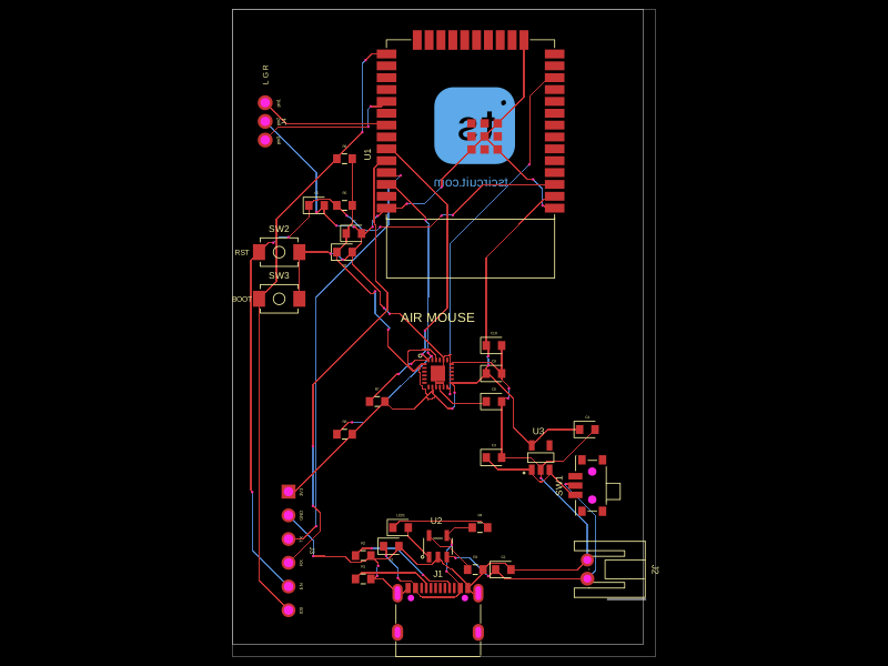 More from this authorhrithik18k/air-mouseThis code defines various surface-mount and through-hole electronic components, specifying their physical footprints, pin configurations, and 3D CAD models for hardware visualization.
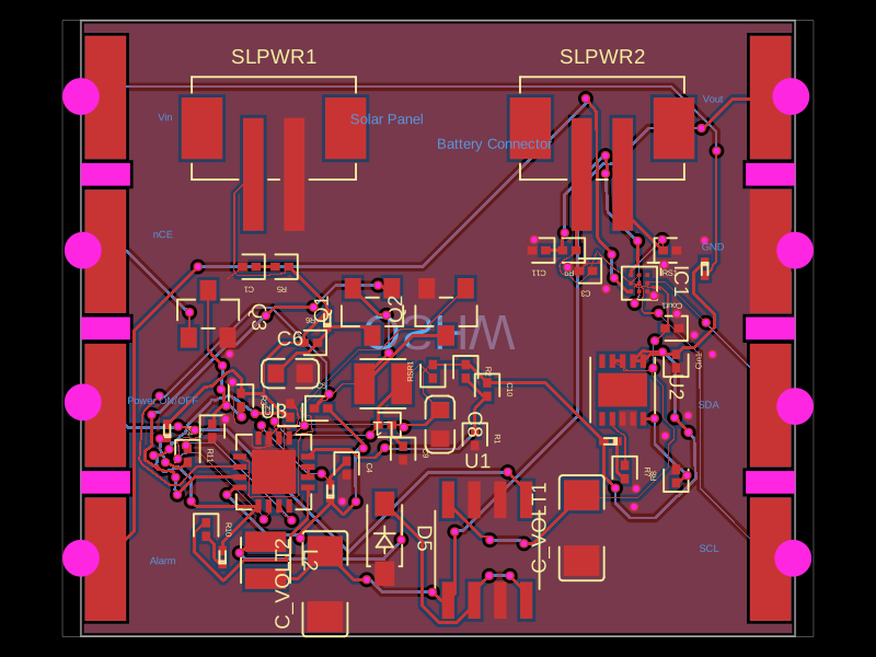 Similar packageShiboSoftwareDev/solar-battery-chargerThis code defines various surface-mount and through-hole electronic components (like diodes, voltage regulators, and ICs) with detailed footprints, 3D models, and pin configurations for PCB design.
 Discover something newShiboSoftwareDev/mspm0g3507-usb-c-dev-boardThe circuit assembles a USB-C port with integrated ESD protection, power regulation, UART interface, and microcontroller (MSPM0G3507) with supporting components for USB data lines, CC termination, I2C, SPI, reset circuitry, and indicator LEDs.