gokul/wireless-calculator
A USB‑C rechargeable battery-powered controller board with MCP73871 Li‑ion charging, TPS63070 buck‑boost and LDO power regulation, ATmega328P and ESP32‑S3 control, LCD/keypad user interface, status LEDs, and UART/programming connectors.
- Version
- 0.0.1
- License
- ISC
- Stars
- 0
dist/fabrication/ASSEMBLY.txt
WIRELESS CALCULATOR — PROTOTYPE FABRICATION RELEASE — 2026-10-23

PCB: 58 x 124 mm, 1.6 mm FR-4, 2 copper layers, nominal 35 um copper.
Smallest routed track 0.15 mm; via drill 0.30 mm / pad 0.60 mm.
Minimum configured track-to-pad clearance 0.15 mm. Copper-to-edge 0.30 mm.
Four mounting holes: 2.20 mm NPTH. JBAT: 0.85 mm finished plated holes.
Use the supplied Excellon drill files. The antenna extends past the board;
do not extend the board outline to include the module's antenna.
Vias are tented by the exported solder mask except where a same-net pad's
mask opening may reach an adjacent via. Review solder-wicking risk at those
locations with the assembler. Inspect QFN exposed-pad paste coverage and
stencil windowing with the assembler before making the stencil.

FILES
wireless-calculator-gerbers.zip: unchanged tscircuit export including copper,
mask, paste, silkscreen, outline, drill files, BOM and full placement table.
wireless-calculator-schematic.pdf: schematic drawing export.
bom.csv: 90 populated components; Comment contains specified manufacturer PN.
pick_and_place.csv: original complete 90-row CLI assembly export.
pick-and-place-smt.csv: 87 rows, excluding LCD1, JBAT and JNTC for hand soldering.
pin-1-orientation-reference.csv: actual board pad coordinates and exported
supplier rotations for checking the assembly preview. Board coordinates are
in mm, origin at board center, +X right / +Y up when viewed from the top.
The supplier rotation column is not the same convention as PCB rotation.
validation.json: versions, checks, artifact hashes and remaining validation.

ASSEMBLY
Hand solder LCD1, JBAT, JNTC after reflow. JISP/JESP are unpopulated access.
Both sides contain SMT parts. LEDs D1/D2/D4 are Lite-On LTST-C190KGKT/C125094;
D3 is LTST-C190KRKT/C94869. Their cathodes are on the right in a top view.
The full exporter warns that some supplier rotations cannot be verified.
Check each polarized part in the supplier placement preview before ordering.
Do not replace MPNs automatically. L1, U5 and U6 generated stock warnings;
verify sourcing or arrange consignment. LCD and battery connector custom
footprints have blank generic Footprint fields in the exported BOM; use the
specified MPN, board drawings and actual pad geometry.

EXTERNAL PARTS
Protected 1S LiPo, 3.7 V nominal, 4.2 V maximum. Example Adafruit 258, 1200 mAh.
JBAT pin 1 positive / pin 2 negative. Verify the battery cable polarity.
Insulated battery-mounted TDK B57371V2103H060 10k NTC assembly to JNTC.
The example battery has no NTC. Do not substitute a fixed resistor.
Battery carrier, insulation, enclosure and keycaps are not included.
Keep metal, battery and wires out of the ESP antenna clearance region.

STATUS
Electrical/layout software checks passed. No physical unit has been tested.
Firmware is not included. This is a prototype manufacturing release, not a
validated production appliance. Perform the power, charge-temperature,
wireless, display and keypad tests described in README.md before production.
Related Packages
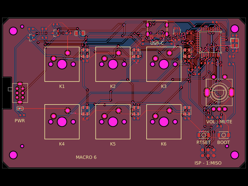 More from this authorgokul/macro-six-usbcUSB-powered ATmega32U4 controller board with protected/switched 5 V power, six tactile keys, rotary encoder, reset/boot/ISP interfaces, power LED, and six daisy-chained SK6812 RGB LEDs driven through MOSFETs.
 Similar packagemohan-bee/esp32-c3This hardware design integrates an ESP32-C3 microcontroller, a USB-C connector, a power management IC (AP2112-3.3V regulator), a USB-to-Serial converter (CH340C), several resistors, capacitors, and user-accessible headers to facilitate USB communication, power regulation, and general I/O interfacing.
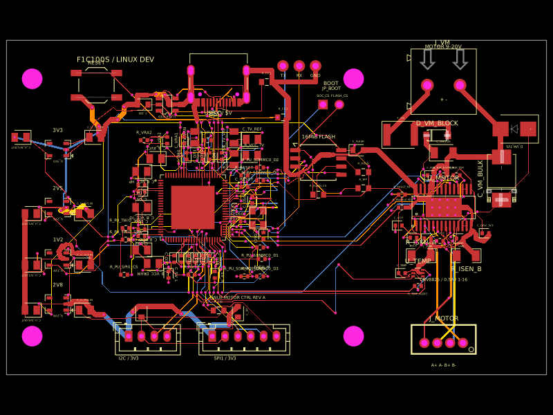 Discover something newShiboSoftwareDev/f1c100s-linux-stepper-controllerA four-layer Linux motor-control carrier built around an Allwinner F1C100S SoC, USB‑C, SPI flash, multi-rail power regulation, DRV8825 stepper-driver stage with protection/current sensing, temperature monitoring, and external I/O connectors.