gokul/usb3-sd-hub
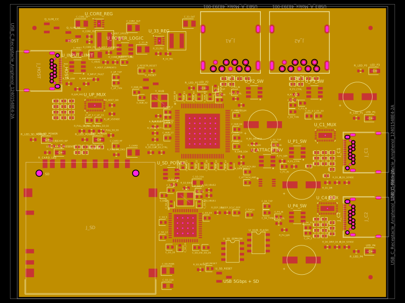
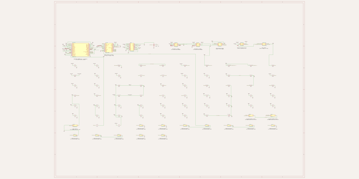
Engineering draft: four-layer, computer-powered USB 3 hub with one USB-C host socket, two USB-C and two USB-A accessory sockets, and a full-size SD slot. Board and three schematic previews are available. Routing and production checks are incomplete; not fabrication ready.
- Version
- 0.1.4
- License
- unset
- Stars
- 0
index.circuit.tsx
PCB
Schematic
import "tscircuit";
import "./design/pcb-position-compatibility";
import "./design/local-solvers";
import "./design/schematic-note-layout";
import "./design/schematic-group-compatibility";
import "./design/schematic-sheet-layout";
import { Fragment } from "react";
import { BoardMarkings } from "./components/BoardMarkings";
import { GroundVias } from "./components/GroundVias";
import { HighSpeedRouting } from "./components/HighSpeedRouting";
import { Controllers } from "./components/Controllers";
import { HostAndPower } from "./sheets/HostAndPower";
import { HubAndPorts } from "./sheets/HubAndPorts";
import { SdReader } from "./sheets/SdReader";

export default () => (
	<board
		name="USB_HUB_BOARD"
		pcbAnchorAlignment="center"
		pcbX="0mm"
		pcbY="0mm"
		width={86}
		height={68}
		layers={4}
		thickness={1.6}
		isViaInPadAllowed
		title="ENGINEERING DRAFT: USB-C / USB-A Hub with Full-size SD"
		autorouter="auto-local"
		schMaxTraceDistance={0.1}
		schAutoLayoutEnabled
		pcbLayout={{ layoutMode: "none" }}
		minTraceWidth={0.136}
		minTraceToPadEdgeClearance={0.13}
		minPadEdgeToPadEdgeClearance={0.13}
		minViaPadDiameter={0.6}
		minViaHoleDiameter={0.3}
		minBoardEdgeClearance={0.3}
		defaultViaTenting="bottom_tented"
		solderMaskColor="black"
		pcbStyle={{ silkscreenFontSize: 0.6 }}
	>
		<net name="GND" isGroundNet nominalTraceWidth={0.4} />
		{["VBUS_HOST", "VBUS_HUB", "VDD12", "VDD33", "SD_VDD33", "CRD_PWR"].map(
			(name) => (
				<Fragment key={name}>
					<net
						name={name}
						isPowerNet
						nominalTraceWidth={name.startsWith("VBUS") ? 0.8 : 0.5}
					/>
				</Fragment>
			),
		)}
		<Controllers />
		<HostAndPower />
		<HubAndPorts />
		<SdReader />
		<GroundVias />
		<HighSpeedRouting />
		<copperpour
			name="GroundReference"
			layer="inner1"
			connectsTo="net.GND"
			unbroken
			clearance={0.2}
			boardEdgeMargin={0.4}
		/>
		<copperpour
			name="GroundBottomReference"
			layer="inner2"
			connectsTo="net.GND"
			unbroken
			clearance={0.2}
			boardEdgeMargin={0.4}
		/>
		<BoardMarkings />
	</board>
);
Related Packages
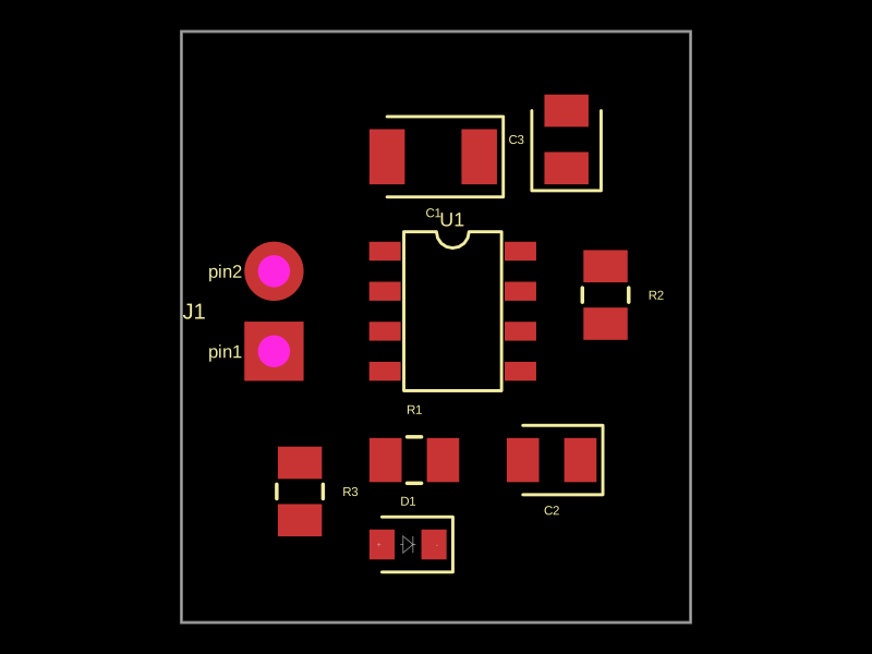 More from this authorgokul/led-blinkingThis design implements a hardware LED blink circuit using a 555 timer IC connected with resistors, capacitors, an LED, and header pins for power input.
 Similar packagepixalynx/usb3-hub-10gA USB 3.2 Gen 2 six-port hub board with USB-C PD power input, regulated 5 V/3.3 V/1.15 V rails, one upstream and four protected downstream USB-A/USB-C ports, SuperSpeed muxes, ESD protection, and controlled port power.
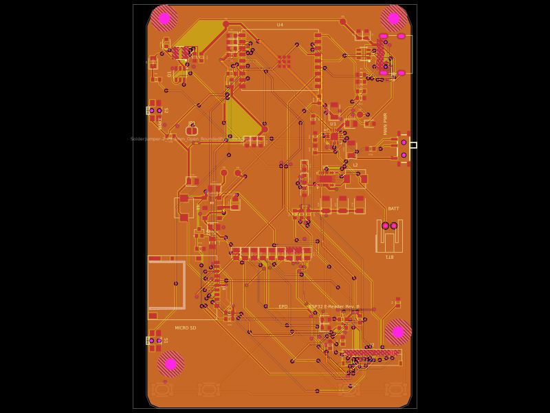 Discover something newrushabhcodes/ESP32-E-ReaderA compact ESP32-C3 board with USB-C power/charging, Li-ion battery protection, 3.3-V regulation, e-paper and microSD interfaces, and user buttons/switches.