gokul/usb3-sd-hub
Engineering draft: four-layer, computer-powered USB 3 hub with one USB-C host socket, two USB-C and two USB-A accessory sockets, and a full-size SD slot. Board and three schematic previews are available. Routing and production checks are incomplete; not fabrication ready.
- Version
- 0.1.4
- License
- unset
- Stars
- 0
imports/SdSocket.tsx
import { Fragment } from "react";
import type { ConnectorProps } from "@tscircuit/props";
import { placementFor } from "../design/placement";

// Hirose DM1AA-SF-PEJ(82), EDC3-153736-02 revision 3, page 1.
// The drawing's mounting-side view uses the left locating hole as its datum.
// Translate that datum to the footprint origin: (11.9 mm, -12.7 mm).
// CD closes on card insertion. WP closes for a write-enabled card.
// Expose the four shell tabs as separate physical ports. They all connect to
// GND, but are too far apart to represent as one short routed pad-to-pad link.
const contactLands = [
	{ pin: "8", x: 1.35 },
	{ pin: "7", x: 3.05 },
	{ pin: "6", x: 5.475 },
	{ pin: "5", x: 7.975 },
	{ pin: "4", x: 10.475 },
	{ pin: "3", x: 12.975 },
	{ pin: "2", x: 15.475 },
	{ pin: "1", x: 17.975 },
	{ pin: "9", x: 20.475 },
];
const switchLands = [
	{ pin: "10", y: -9.2 },
	{ pin: "11", y: -18.15 },
	{ pin: "12", y: -20.75 },
];
const shellLands = [
	{ x: -2.6, y: -4.55 },
	{ x: 26.4, y: -4.55 },
	{ x: -2.2, y: -23.2 },
	{ x: 26.4, y: -23.2 },
];

export const SdSocket = (props: ConnectorProps) => (
	<connector
		pinAttributes={{
			pin3: { requiresGround: true },
			pin6: { requiresGround: true },
			pin12: { requiresGround: true },
			pin13: { requiresGround: true },
			pin14: { requiresGround: true },
			pin15: { requiresGround: true },
			pin16: { requiresGround: true },
			pin4: {
				requiresPower: true,
				requiresVoltage: "3.3V",
				requiredVoltageTolerance: "10%",
			},
		}}
		footprint={
			<footprint insertionDirection="from_bottom">
				{contactLands.map((land) => (
					<Fragment key={land.pin}>
						<smtpad
							portHints={[land.pin]}
							pcbX={`${land.x - 11.9}mm`}
							pcbY="14.9mm"
							width="1.1mm"
							height="2mm"
							shape="rect"
							layer="top"
						/>
					</Fragment>
				))}
				{switchLands.map((land) => (
					<Fragment key={land.pin}>
						<smtpad
							portHints={[land.pin]}
							pcbX="-14.1mm"
							pcbY={`${land.y + 12.7}mm`}
							width="2mm"
							height="1mm"
							shape="rect"
							layer="top"
						/>
					</Fragment>
				))}
				{shellLands.map((land, index) => (
					<Fragment key={index}>
						<smtpad
							portHints={[`${index + 13}`]}
							pcbX={`${land.x - 11.9}mm`}
							pcbY={`${land.y + 12.7}mm`}
							width="2mm"
							height="2mm"
							shape="rect"
							layer="top"
						/>
					</Fragment>
				))}
				<hole pcbX="-11.9mm" pcbY="12.7mm" diameter="1.3mm" />
				<hole pcbX="10.5mm" pcbY="12.7mm" diameter="1.3mm" />
				<courtyardrect
					pcbX="0mm"
					pcbY="0.1mm"
					width="31.6mm"
					height="32.1mm"
					layer="top"
				/>
				<fabricationnoterect
					pcbX="0mm"
					pcbY="0mm"
					width="30mm"
					height="30.5mm"
					strokeWidth="0.1mm"
				/>
				<fabricationnotetext
					text={props.name ?? ""}
					pcbX="0mm"
					pcbY="0mm"
					fontSize="1mm"
				/>
				<silkscreenline
					x1="-15.2mm"
					y1="-15.45mm"
					x2="15.2mm"
					y2="-15.45mm"
					strokeWidth="0.12mm"
				/>
				<silkscreenline
					x1="-15.2mm"
					y1="-15.45mm"
					x2="-15.2mm"
					y2="-12mm"
					strokeWidth="0.12mm"
				/>
				<silkscreenline
					x1="15.2mm"
					y1="-15.45mm"
					x2="15.2mm"
					y2="-12mm"
					strokeWidth="0.12mm"
				/>
			</footprint>
		}
		cadModel={{
			jscad: { type: "cuboid", size: [30, 30.5, 2.9] },
			zOffsetFromSurface: 1.45,
		}}
		{...props}
		{...placementFor(props.name)}
	/>
);
Related Packages
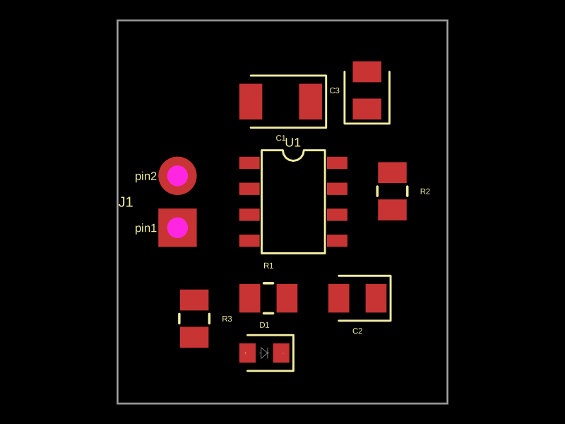 More from this authorgokul/led-blinkingThis design implements a hardware LED blink circuit using a 555 timer IC connected with resistors, capacitors, an LED, and header pins for power input.
 Similar packagepixalynx/usb3-hub-10gA USB 3.2 Gen 2 six-port hub board with USB-C PD power input, regulated 5 V/3.3 V/1.15 V rails, one upstream and four protected downstream USB-A/USB-C ports, SuperSpeed muxes, ESD protection, and controlled port power.
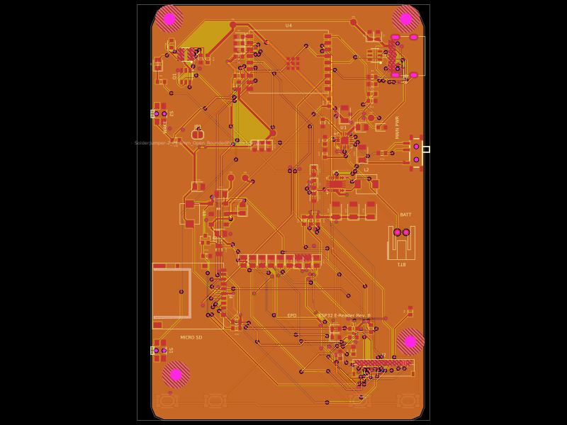 Discover something newrushabhcodes/ESP32-E-ReaderA compact ESP32-C3 board with USB-C power/charging, Li-ion battery protection, 3.3-V regulation, e-paper and microSD interfaces, and user buttons/switches.