gokul/six-digit-logic-clock
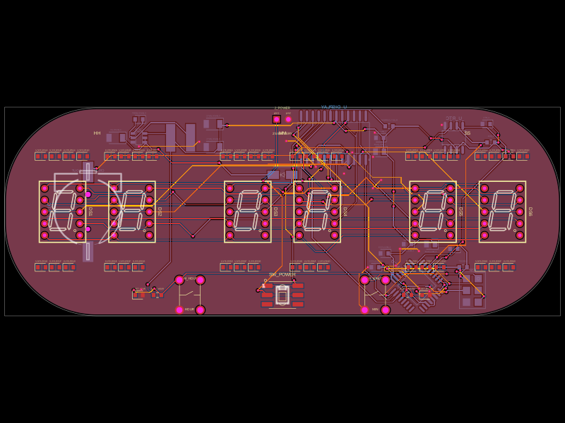
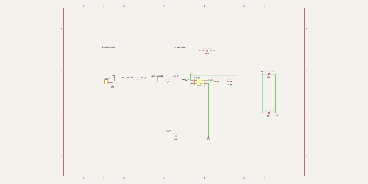
This code defines the physical layout and schematic connections for a multi-layer PCB featuring components like RTC modules (DS3231MZ), microcontroller (ATMEGA328P), LED display driver (MAX7219), and various passive and discrete components, with detailed footprints, pinouts, and placement for a clock and control interface.
- Version
- 0.1.2
- License
- unset
- Stars
- 0
index.circuit.tsx
PCB
Schematic
import { FJ3191AH } from "./imports/c44296"
import { YTSPS_22E58LM } from "./imports/c2941005"
import { ATMEGA328P_AU } from "./imports/c14877"
import { MAX7219EWG_T } from "./imports/c52476"
import { DS3231MZ_TRL } from "./imports/c107410"
import { CR1220_2 } from "./imports/c70381"

const segments = ["A", "B", "C", "D", "E", "F", "G"] as const

const jlc = (partNumber: string) => ({ jlcpcb: [partNumber] })

const digits = [
  { display: "DS1", role: "H10", x: -47.5, digitNet: "DIG5" },
  { display: "DS2", role: "H1", x: -32.5, digitNet: "DIG4" },
  { display: "DS3", role: "M10", x: -7.5, digitNet: "DIG3" },
  { display: "DS4", role: "M1", x: 7.5, digitNet: "DIG2" },
  { display: "DS5", role: "S10", x: 32.5, digitNet: "DIG1" },
  { display: "DS6", role: "S1", x: 47.5, digitNet: "DIG0" },
] as const

const digitSchPositionByRole = {
  H10: { x: -8, y: 4 },
  H1: { x: -8, y: -4 },
  M10: { x: 0, y: 4 },
  M1: { x: 0, y: -4 },
  S10: { x: 8, y: 4 },
  S1: { x: 8, y: -4 },
} as const

function DisplayDigit({ display, role, x, digitNet }: (typeof digits)[number]) {
  const resistorX = [x - 4.5, x - 1.5, x + 1.5, x + 4.5]
  return (
    <>
      <FJ3191AH
        name={display}
        pcbX={x}
        pcbY={0}
        pcbRotation="270deg"
        schX={digitSchPositionByRole[role].x}
        schY={digitSchPositionByRole[role].y}
        schSheetName="display_digits"
        noConnect={["dp"]}
        connections={{
          GND1: `net.${digitNet}`,
          GND2: `net.${digitNet}`,
          a: "net.SEG_A",
          b: "net.SEG_B",
          c: "net.SEG_C",
          d: "net.SEG_D",
          e: "net.SEG_E",
          f: "net.SEG_F",
          g: "net.SEG_G",
        }}
      />

      {/* The original front-side 0 ohm resistor footprints stay populated in
          the exact same positions for the visual design. MAX7219 regulates
          segment current, so these visual links intentionally float and are
          not in the signal path. */}
      {segments.map((segment, index) => (
        <chip
          key={`${display}-${segment}`}
          name={`U_VIS_${display}_${segment}`}
          manufacturerPartNumber="0OHM-VISUAL-LINK"
          footprint="0603"
          supplierPartNumbers={jlc("C21189")}
          pcbX={resistorX[index % 4]}
          pcbY={index < 4 ? 12 : -12}
          pinLabels={{ pin1: ["1"], pin2: ["2"] }}
          noSchematicRepresentation
          noConnect={["pin1", "pin2"]}
        />
      ))}
    </>
  )
}

const atmegaPinLabels = {
  pin1: ["PD3_HOUR"], pin2: ["PD4"], pin3: ["GND1"], pin4: ["VCC1"],
  pin5: ["GND2"], pin6: ["VCC2"], pin7: ["PB6_XTAL1"], pin8: ["PB7_XTAL2"],
  pin9: ["PD5"], pin10: ["PD6"], pin11: ["PD7"], pin12: ["PB0"],
  pin13: ["PB1"], pin14: ["PB2_LOAD"], pin15: ["PB3_MOSI"], pin16: ["PB4_MISO"],
  pin17: ["PB5_SCK"], pin18: ["AVCC"], pin19: ["ADC6"], pin20: ["AREF"],
  pin21: ["GND3"], pin22: ["ADC7"], pin23: ["PC0"], pin24: ["PC1"],
  pin25: ["PC2"], pin26: ["PC3"], pin27: ["PC4_SDA"], pin28: ["PC5_SCL"],
  pin29: ["N_RESET"], pin30: ["PD0_RX"], pin31: ["PD1_TX"], pin32: ["PD2_MINUTE"],
} as const

const maxPinLabels = {
  pin1: ["DIN"], pin2: ["DIG0"], pin3: ["DIG4"], pin4: ["GND1"],
  pin5: ["DIG6"], pin6: ["DIG2"], pin7: ["DIG3"], pin8: ["DIG7"],
  pin9: ["GND2"], pin10: ["DIG5"], pin11: ["DIG1"], pin12: ["LOAD"],
  pin13: ["CLK"], pin14: ["SEG_A"], pin15: ["SEG_F"], pin16: ["SEG_B"],
  pin17: ["SEG_G"], pin18: ["ISET"], pin19: ["V5"], pin20: ["SEG_C"],
  pin21: ["SEG_E"], pin22: ["SEG_DP"], pin23: ["SEG_D"], pin24: ["DOUT"],
} as const

const ispPinLabels = {
  pin1: ["MISO"], pin2: ["V5"], pin3: ["SCK"],
  pin4: ["MOSI"], pin5: ["RESET"], pin6: ["GND"],
} as const

const ispFootprint = (
  <footprint>
    <smtpad portHints={["pin1"]} pcbX={-1.27} pcbY={2.54} width="1.6mm" height="1.6mm" shape="rect" />
    <smtpad portHints={["pin2"]} pcbX={1.27} pcbY={2.54} width="1.6mm" height="1.6mm" shape="rect" />
    <smtpad portHints={["pin3"]} pcbX={-1.27} pcbY={0} width="1.6mm" height="1.6mm" shape="rect" />
    <smtpad portHints={["pin4"]} pcbX={1.27} pcbY={0} width="1.6mm" height="1.6mm" shape="rect" />
    <smtpad portHints={["pin5"]} pcbX={-1.27} pcbY={-2.54} width="1.6mm" height="1.6mm" shape="rect" />
    <smtpad portHints={["pin6"]} pcbX={1.27} pcbY={-2.54} width="1.6mm" height="1.6mm" shape="rect" />
    <silkscreenrect pcbX={0} pcbY={0} width="5.6mm" height="7.9mm" />
    <silkscreencircle pcbX={-1.27} pcbY={2.54} radius="0.3mm" />
  </footprint>
)

export default function ClockBoard() {
  return (
    <board
      name="CLOCKBOARD"
      width="120mm"
      height="45mm"
      borderRadius="20mm"
      layers={4}
      thickness="1.6mm"
      title="Six Digit RTC Clock - Fabrication Revision"
      minViaHoleDiameter="0.3mm"
      minViaPadDiameter="0.6mm"
      minViaEdgeToPadEdgeClearance="0.09mm"
      minTraceToPadEdgeClearance="0.07mm"
      defaultTraceWidth="0.2mm"
      schLayout={{ layoutMode: "relative" }}
      schTraceAutoLabelEnabled
      schMaxTraceDistance={0.5}
      autorouter={{
        preset: "tscircuit_beta",
        allowViaInPad: false,
        traceClearance: "0.25mm",
        serverCacheEnabled: false,
      }}
    >
      <schematicsheet name="power" displayName="1 - Power Input and 5V Buck" sheetIndex={0}>
        <schematicsection name="entry" displayName="2S BATTERY INPUT" />
        <schematicsection name="buck" displayName="5V BUCK SUPPLY" />

        <pinheader
          name="J_POWER"
          pinCount={2}
          pitch="2.54mm"
          footprint="pinrow2_p2.54"
          pcbX={0}
          pcbY={20}
          schX={-11}
          schY={3}
          schSectionName="entry"
          connections={{ pin1: "net.VBAT_2S", pin2: "net.GND" }}
        />
        <YTSPS_22E58LM
          name="SW_POWER"
          pcbX={0}
          pcbY={-18}
          layer="top"
          schX={-7}
          schY={3}
          schSectionName="entry"
          noConnect={["pin3", "pin6"]}
          connections={{
            pin2: "net.VBAT_2S", pin5: "net.VBAT_2S",
            pin1: "net.VBAT_SWITCHED", pin4: "net.VBAT_SWITCHED",
          }}
        />
        <diode
          name="D_REVERSE"
          manufacturerPartNumber="SS34"
          supplierPartNumbers={{ jlcpcb: ["C8678"] }}
          footprint="sma"
          pcbX={0}
          pcbY={8}
          layer="bottom"
          schX={-3}
          schY={3}
          schSectionName="entry"
          connections={{ anode: "net.VBAT_SWITCHED", cathode: "net.VBAT_SW" }}
        />

        <chip
          name="U_BUCK"
          manufacturerPartNumber="AP63205WU-7"
          supplierPartNumbers={{ jlcpcb: ["C2071056"] }}
          footprint="sot23_6"
          pinLabels={{
            pin1: ["FB"], pin2: ["EN"], pin3: ["VIN"],
            pin4: ["GND"], pin5: ["SW"], pin6: ["BST"],
          }}
          pinAttributes={{ pin3: { requiresPower: true }, pin4: { requiresGround: true } }}
          pcbX={-31}
          pcbY={16}
          layer="bottom"
          schX={1}
          schY={3}
          schSectionName="buck"
          connections={{
            FB: "net.V5", EN: "net.VBAT_SW", VIN: "net.VBAT_SW",
            GND: "net.GND", SW: "net.BUCK_SW", BST: "net.BUCK_BST",
          }}
        />
        <capacitor
          name="C_BUCK_IN"
          capacitance="10uF"
          manufacturerPartNumber="TCC1206X7R106K250HT"
          supplierPartNumbers={{ jlcpcb: ["C380364"] }}
          footprint="1206"
          pcbX={-36}
          pcbY={16}
          layer="bottom"
          schX={-2}
          schY={-4}
          schSectionName="buck"
          connections={{ pin1: "net.VBAT_SW", pin2: "net.GND" }}
        />
        <capacitor
          name="C_BUCK_BOOT"
          capacitance="100nF"
          supplierPartNumbers={jlc("C14663")}
          footprint="0603"
          pcbX={-31}
          pcbY={20}
          layer="bottom"
          schX={2}
          schY={7}
          schSectionName="buck"
          connections={{ pin1: "net.BUCK_BST", pin2: "net.BUCK_SW" }}
        />
        <inductor
          name="L_BUCK"
          manufacturerPartNumber="SRN6045TA-4R7M"
          supplierPartNumbers={{ jlcpcb: ["C2044594"] }}
          inductance="4.7uH"
          pcbX={-22}
          pcbY={16}
          layer="bottom"
          schX={5}
          schY={3}
          schSectionName="buck"
          footprint={
            <footprint>
              <smtpad portHints={["pin1"]} pcbX={-2.15} pcbY={0} width="2mm" height="6mm" shape="rect" />
              <smtpad portHints={["pin2"]} pcbX={2.15} pcbY={0} width="2mm" height="6mm" shape="rect" />
              <courtyardoutline outline={[
                { x: -3.5, y: -3.5 }, { x: 3.5, y: -3.5 },
                { x: 3.5, y: 3.5 }, { x: -3.5, y: 3.5 },
                { x: -3.5, y: -3.5 },
              ]} />
            </footprint>
          }
          connections={{ pin1: "net.BUCK_SW", pin2: "net.V5" }}
        />
        <capacitor
          name="C_BUCK_OUT1"
          capacitance="22uF"
          supplierPartNumbers={jlc("C12891")}
          footprint="1206"
          pcbX={-15}
          pcbY={14}
          layer="bottom"
          schX={10}
          schY={4}
          schSectionName="buck"
          connections={{ pin1: "net.V5", pin2: "net.GND" }}
        />
        <capacitor
          name="C_BUCK_OUT2"
          capacitance="22uF"
          supplierPartNumbers={jlc("C12891")}
          footprint="1206"
          pcbX={-15}
          pcbY={19}
          layer="bottom"
          schX={10}
          schY={-1}
          schSectionName="buck"
          connections={{ pin1: "net.V5", pin2: "net.GND" }}
        />
      </schematicsheet>

      <schematicsheet name="controller" displayName="2 - Controller and Programming" sheetIndex={1}>
        <schematicsection name="mcu" displayName="ATMEGA328P CONTROLLER" />
        <schematicsection name="programming" displayName="AVR ICSP PROGRAMMING" />

        <ATMEGA328P_AU
          name="U_MCU"
          pinLabels={atmegaPinLabels}
          pcbX={29}
          pcbY={-16}
          pcbRotation="45deg"
          layer="bottom"
          schX={-5}
          schY={2}
          schSectionName="mcu"
          noConnect={[
            "PD4", "PB6_XTAL1", "PB7_XTAL2", "PD5", "PD6", "PD7", "PB0", "PB1",
            "ADC6", "ADC7", "PC0", "PC1", "PC2", "PC3", "PD0_RX", "PD1_TX",
          ]}
          connections={{
            GND1: "net.GND", GND2: "net.GND", GND3: "net.GND",
            VCC1: "net.V5", VCC2: "net.V5", AVCC: "net.V5",
            AREF: "net.AREF",
            PD3_HOUR: "net.HOUR_BUTTON",
            PD2_MINUTE: "net.MINUTE_BUTTON",
            PB2_LOAD: "net.MAX_LOAD",
            PB3_MOSI: "net.MAX_DIN",
            PB4_MISO: "net.ISP_MISO",
            PB5_SCK: "net.MAX_CLK",
            PC4_SDA: "net.I2C_SDA",
            PC5_SCL: "net.I2C_SCL",
            N_RESET: "net.MCU_RESET",
          }}
        />
        <capacitor name="C_MCU_VCC1" capacitance="100nF" supplierPartNumbers={jlc("C14663")} footprint="0603" pcbX={20} pcbY={-12} layer="bottom" schX={-11} schY={-6} schSectionName="mcu" connections={{ pin1: "net.V5", pin2: "net.GND" }} />
        <capacitor name="C_MCU_VCC2" capacitance="100nF" supplierPartNumbers={jlc("C14663")} footprint="0603" pcbX={22} pcbY={-9} layer="bottom" schX={-8} schY={-6} schSectionName="mcu" connections={{ pin1: "net.V5", pin2: "net.GND" }} />
        <capacitor name="C_MCU_AVCC" capacitance="100nF" supplierPartNumbers={jlc("C14663")} footprint="0603" pcbX={27} pcbY={-7} layer="bottom" schX={-5} schY={-6} schSectionName="mcu" connections={{ pin1: "net.V5", pin2: "net.GND" }} />
        <capacitor name="C_MCU_BULK" capacitance="4.7uF" supplierPartNumbers={jlc("C1779")} footprint="0805" pcbX={32} pcbY={-7} layer="bottom" schX={-2} schY={-6} schSectionName="mcu" connections={{ pin1: "net.V5", pin2: "net.GND" }} />
        <capacitor name="C_AREF" capacitance="100nF" supplierPartNumbers={jlc("C14663")} footprint="0603" pcbX={37} pcbY={-8} layer="bottom" schX={1} schY={-6} schSectionName="mcu" connections={{ pin1: "net.AREF", pin2: "net.GND" }} />
        <resistor name="R_RESET" resistance="10kohm" supplierPartNumbers={jlc("C25804")} footprint="0603" pcbX={39} pcbY={-12} layer="bottom" schX={0} schY={6} schSectionName="mcu" connections={{ pin1: "net.V5", pin2: "net.MCU_RESET" }} />

        <DS3231MZ_TRL
          name="U_RTC"
          pcbX={37}
          pcbY={16}
          layer="bottom"
          schX={-8}
          schY={4}
          schSheetName="rtc_driver"
          schSectionName="rtc"
          noConnect={["32kHz", "pin3", "N_RST"]}
          connections={{
            VCC: "net.V5", GND: "net.GND", VBAT: "net.RTC_BAT",
            SDA: "net.I2C_SDA", SCL: "net.I2C_SCL",
          }}
        />
        <CR1220_2
          name="BT_RTC"
          pcbX={-42}
          pcbY={0}
          pcbRotation="90deg"
          layer="bottom"
          schX={-12}
          schY={4}
          schSheetName="rtc_driver"
          schSectionName="rtc"
          connections={{ pin1: "net.RTC_BAT", pin2: "net.GND" }}
        />
        <capacitor name="C_RTC" capacitance="100nF" supplierPartNumbers={jlc("C14663")} footprint="0603" pcbX={44} pcbY={19} layer="bottom" schX={-8} schY={0} schSheetName="rtc_driver" schSectionName="rtc" connections={{ pin1: "net.V5", pin2: "net.GND" }} />
        <resistor name="R_SDA" resistance="4.7kohm" supplierPartNumbers={jlc("C23162")} footprint="0603" pcbX={45} pcbY={15} layer="bottom" schX={-3} schY={5} schSheetName="rtc_driver" schSectionName="rtc" connections={{ pin1: "net.V5", pin2: "net.I2C_SDA" }} />
        <resistor name="R_SCL" resistance="4.7kohm" supplierPartNumbers={jlc("C23162")} footprint="0603" pcbX={49} pcbY={12} layer="bottom" schX={-3} schY={2} schSheetName="rtc_driver" schSectionName="rtc" connections={{ pin1: "net.V5", pin2: "net.I2C_SCL" }} />

        <pushbutton
          name="SW_HOUR"
          footprint="pushbutton_id1.3mm_od2mm"
          pcbX={-20}
          pcbY={-18}
          layer="top"
          schX={-10}
          schY={-4}
          schSheetName="rtc_driver"
          schSectionName="controls"
          noConnect={["pin3", "pin4"]}
          connections={{ pin1: "net.HOUR_BUTTON", pin2: "net.GND" }}
        />
        <resistor name="R_SET_HOUR" resistance="10kohm" supplierPartNumbers={jlc("C25804")} footprint="0603" pcbX={-27} pcbY={-18} layer="top" schX={-13} schY={-4} schSheetName="rtc_driver" schSectionName="controls" connections={{ pin1: "net.V5", pin2: "net.HOUR_BUTTON" }} />
        <capacitor name="C_SET_HOUR" capacitance="100nF" supplierPartNumbers={jlc("C14663")} footprint="0603" pcbX={-31} pcbY={-18} layer="top" schX={-10} schY={-7} schSheetName="rtc_driver" schSectionName="controls" connections={{ pin1: "net.HOUR_BUTTON", pin2: "net.GND" }} />

        <pushbutton
          name="SW_MINUTE"
          footprint="pushbutton_id1.3mm_od2mm"
          pcbX={20}
          pcbY={-18}
          layer="top"
          schX={-3}
          schY={-4}
          schSheetName="rtc_driver"
          schSectionName="controls"
          noConnect={["pin3", "pin4"]}
          connections={{ pin1: "net.MINUTE_BUTTON", pin2: "net.GND" }}
        />
        <resistor name="R_SET_MINUTE" resistance="10kohm" supplierPartNumbers={jlc("C25804")} footprint="0603" pcbX={27} pcbY={-18} layer="top" schX={-6} schY={-4} schSheetName="rtc_driver" schSectionName="controls" connections={{ pin1: "net.V5", pin2: "net.MINUTE_BUTTON" }} />
        <capacitor name="C_SET_MINUTE" capacitance="100nF" supplierPartNumbers={jlc("C14663")} footprint="0603" pcbX={31} pcbY={-18} layer="top" schX={-3} schY={-7} schSheetName="rtc_driver" schSectionName="controls" connections={{ pin1: "net.MINUTE_BUTTON", pin2: "net.GND" }} />

        <chip
          name="J_ICSP"
          manufacturerPartNumber="AVR-ISP-POGO-PADS"
          footprint={ispFootprint}
          pinLabels={ispPinLabels}
          pcbX={41}
          pcbY={-17}
          layer="bottom"
          schX={7}
          schY={-1}
          schSheetName="controller"
          schSectionName="programming"
          connections={{
            MISO: "net.ISP_MISO", V5: "net.V5", SCK: "net.MAX_CLK",
            MOSI: "net.MAX_DIN", RESET: "net.MCU_RESET", GND: "net.GND",
          }}
        />
      </schematicsheet>

      <schematicsheet name="rtc_driver" displayName="3 - RTC, Controls and Display Driver" sheetIndex={2}>
        <schematicsection name="rtc" displayName="DS3231M RTC + CR1220 BACKUP" />
        <schematicsection name="controls" displayName="HOUR / MINUTE BUTTONS" />
        <schematicsection name="driver" displayName="MAX7219 DRIVER" />

        <MAX7219EWG_T
          name="U_DISPLAY"
          pinLabels={maxPinLabels}
          pcbX={11}
          pcbY={16}
          layer="bottom"
          schX={6}
          schY={1}
          schSectionName="driver"
          noConnect={["DIG6", "DIG7", "SEG_DP", "DOUT"]}
          connections={{
            DIN: "net.MAX_DIN", LOAD: "net.MAX_LOAD", CLK: "net.MAX_CLK",
            GND1: "net.GND", GND2: "net.GND", V5: "net.V5", ISET: "net.MAX_ISET",
            DIG0: "net.DIG0", DIG1: "net.DIG1", DIG2: "net.DIG2",
            DIG3: "net.DIG3", DIG4: "net.DIG4", DIG5: "net.DIG5",
            SEG_A: "net.SEG_A", SEG_B: "net.SEG_B", SEG_C: "net.SEG_C",
            SEG_D: "net.SEG_D", SEG_E: "net.SEG_E", SEG_F: "net.SEG_F", SEG_G: "net.SEG_G",
          }}
        />
        <resistor name="R_SET_CURRENT" resistance="82kohm" supplierPartNumbers={jlc("C23254")} footprint="0603" pcbX={23} pcbY={18.5} layer="bottom" schX={12} schY={5} schSectionName="driver" connections={{ pin1: "net.V5", pin2: "net.MAX_ISET" }} />
        <capacitor name="C_MAX_LOCAL" capacitance="100nF" supplierPartNumbers={jlc("C14663")} footprint="0603" pcbX={21} pcbY={16} layer="bottom" schX={7} schY={-6} schSectionName="driver" connections={{ pin1: "net.V5", pin2: "net.GND" }} />
        <capacitor name="C_MAX_BULK" capacitance="10uF" supplierPartNumbers={jlc("C15850")} footprint="0805" pcbX={21} pcbY={13} layer="bottom" schX={12} schY={-6} schSectionName="driver" connections={{ pin1: "net.V5", pin2: "net.GND" }} />

        {digits.map((digit) => <DisplayDigit key={digit.display} {...digit} />)}
      </schematicsheet>

      <schematicsheet name="display_digits" displayName="4 - Six-Digit LED Display" sheetIndex={3}>
        <schematictext text="HOURS" schX={-8} schY={8} fontSize={0.45} />
        <schematictext text="MINUTES" schX={0} schY={8} fontSize={0.45} />
        <schematictext text="SECONDS" schX={8} schY={8} fontSize={0.45} />
      </schematicsheet>

      {/* The front-side outline, placements, labels and visual composition are unchanged. */}
      <silkscreentext text="HH" pcbX={-40} pcbY={17} fontSize="1mm" />
      <silkscreentext text="MM" pcbX={0} pcbY={17} fontSize="1mm" />
      <silkscreentext text="SS" pcbX={40} pcbY={17} fontSize="1mm" />
      <silkscreentext text="HOUR" pcbX={-20} pcbY={-21} fontSize="0.7mm" />
      <silkscreentext text="MIN" pcbX={20} pcbY={-21} fontSize="0.7mm" />
      <silkscreentext text="2S BATTERY" pcbX={0} pcbY={17} fontSize="0.7mm" />

      <silkscreentext text="CR1220 + FACE OUT" pcbX={-42} pcbY={9} layer="bottom" fontSize="0.7mm" />
      <silkscreentext text="ICSP" pcbX={41} pcbY={-12.5} layer="bottom" fontSize="0.7mm" />

      <copperpour connectsTo="net.GND" layer="top" clearance="0.2mm" boardEdgeMargin="0.3mm" />
      <copperpour connectsTo="net.GND" layer="bottom" clearance="0.2mm" boardEdgeMargin="0.3mm" />
    </board>
  )
}
Related Packages
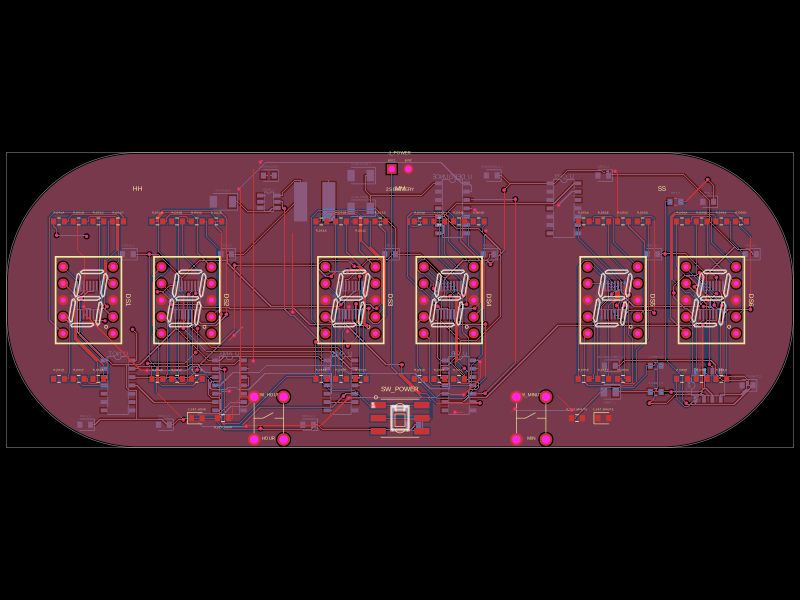 More from this authorgokul/new-clockThis code defines a PCB schematic with physical hardware components including switches, chips, resistors, capacitors, inductors, connectors, and visual annotations for a six-digit 12-hour digital clock circuit.
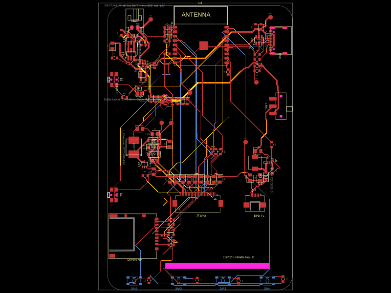 Similar packagerushabhcodes/ESP32-E-ReaderThis code defines the hardware layout and schematic connections for an ESP32-based e-reader device, including microcontroller, USB, display, power management, connectors, passives, switches, and associated PCB footprints, placements, and net connections.