gokul/six-digit-logic-clock
This code defines the physical layout and schematic connections for a multi-layer PCB featuring components like RTC modules (DS3231MZ), microcontroller (ATMEGA328P), LED display driver (MAX7219), and various passive and discrete components, with detailed footprints, pinouts, and placement for a clock and control interface.
- Version
- 0.1.2
- License
- unset
- Stars
- 0
FABRICATION.md
# Six-Digit RTC Clock - Fabrication and Bring-Up Notes

## Release status

This revision is ready for a **prototype fabrication run**. The generated
four-layer board has 32 electrical nets, 131 routed traces, 91 vias, no jumpers,
and zero errors from both the tscircuit build and a separate
`@tscircuit/checks` pass.

Do not move the front displays, buttons, switch, labels, or the capsule outline.
The 42 front-side 0603 zero-ohm parts are retained in their original locations
for appearance only. Both pads are intentionally unconnected; the MAX7219 drives
the LED segments directly and regulates their current through R_SET_CURRENT.

## PCB order

- Shape/size: 120 mm x 45 mm capsule, 20 mm corner radius
- Stackup: 4 layers, 1.6 mm FR-4
- Copper: 1 oz outer and inner layers is sufficient for this clock load
- Surface finish: lead-free HASL or ENIG
- Solder mask: any color; verify small-silkscreen readability in the fab preview
- Minimum routed trace: 0.20 mm
- Routed via: 0.60 mm pad / 0.30 mm finished hole
- Ground pours: top and bottom, 0.20 mm clearance, 0.30 mm board-edge margin
- Assembly: parts on both sides; displays and controls are on top, logic and
  power parts are mainly on bottom

Four layers are the honest choice for this fixed front layout. A skilled manual
router could probably force a two-layer version, but the display pins and 42
locked visual footprints leave narrow channels and long shared segment buses.
The four-layer result routes cleanly without enlarging the board and gives much
better return-current paths. Increasing the board size is not necessary.

## Electrical limits

- J_POWER pin 1: protected 2-cell Li-ion input, 6.0 V to 8.4 V
- J_POWER pin 2: GND
- Do not connect a bare/unprotected cell pack.
- Do not feed 5 V into J_POWER; the AP63205 stage is designed here for a 2S pack.
- D_REVERSE (SS34) provides series reverse-polarity protection. It is not a
  replacement for battery over-current, over-charge, or under-voltage protection.
- This board is a low-current clock. It is not released as a general-purpose 2 A
  AP63205 power module even though the regulator IC is rated up to 2 A.

## Key assembly parts

| Function | Reference | Part | LCSC/JLCPCB |
| --- | --- | --- | --- |
| MCU | U_MCU | ATmega328P-AU, TQFP-32 | C14877 |
| RTC | U_RTC | DS3231MZ+TRL | C107410 |
| LED driver | U_DISPLAY | MAX7219EWG+T | C52476 |
| LED peak-current setting | R_SET_CURRENT | 82 kOhm / 0603 | C23254 |
| 5 V buck | U_BUCK | AP63205WU-7 | C2071056 |
| Buck inductor | L_BUCK | SRN6045TA-4R7M, 4.7 uH | C2044594 |
| Reverse protection | D_REVERSE | SS34 | C8678 |
| Displays | DS1-DS6 | FJ3191AH, common cathode | C44296 |
| RTC cell holder | BT_RTC | CR1220 holder | C70381 |
| 100 nF / 0603 | local bypass capacitors | 50 V X7R | C14663 |
| 4.7 uF / 0805 | C_MCU_BULK | 25 V X5R | C1779 |
| 10 uF / 0805 | C_MAX_BULK | 25 V X5R | C15850 |
| 0 ohm / 0603 | 42 visual front links | 0603 jumper | C21189 |

Stock changes. Recheck every supplier code and placement rotation in the
assembler's live quote before paying. In particular, verify the exact mechanical
variant of the power switch, pushbuttons, power connector, and CR1220 holder
against the parts you will actually buy.

## Programming

Use the six bottom ICSP pogo pads:

1. MISO
2. +5 V
3. SCK
4. MOSI
5. RESET
6. GND

Recommended MiniCore settings:

- MCU: ATmega328P
- Clock: internal 8 MHz
- Brown-out detection: 2.7 V
- EEPROM: retained
- Programmer: your connected AVR ISP

Flash `clock_firmware.ino`. On the first start, or after the RTC reports an
oscillator-stop condition, the firmware writes the compile date/time to the RTC.
The HOUR and MIN buttons then adjust the displayed 24-hour time. A CR1220 keeps
the RTC running when the main battery is switched off.

## Bring-up checklist

1. Inspect the assembler's Gerber, drill, solder-paste, and pick-and-place previews.
2. With no ICs powered, check J_POWER for a short to GND.
3. Apply 6.0 V from a current-limited bench supply at about 100 mA.
4. Confirm correct polarity after D_REVERSE and 5.0 V at the buck output.
5. Increase the current limit only after the 5 V rail is stable.
6. Program the MCU over ICSP and verify all six digits.
7. Check HOUR and MIN buttons and confirm the RTC retains time with main power off.
8. Build 3-5 prototypes and run them for at least 24 hours before a volume order.

## Known engineering caveats

- ATmega328P is marked "Not Recommended for New Designs" by Microchip. It is
  still functional and supported here, but a future volume revision should use a
  current AVR family if long-term sourcing matters.
- The MAX7219 current-set value is 82 kOhm, chosen conservatively for the
  FJ3191AH display's published 8 mA forward-current value. Firmware starts at
  moderate digital brightness. Confirm readability and temperature on the first
  prototypes; do not reduce R_SET_CURRENT without checking peak LED current.
- The CR1220 holder's `+ FACE OUT` silkscreen is intentional. Verify holder pin 1
  is positive in the exact purchased part before assembly.
- The AP63205 input capacitor, bootstrap capacitor, inductor, and output
  capacitors are kept close on the bottom side. Do not treat the board as a 2 A
  reference layout without thermal/current testing.
Related Packages
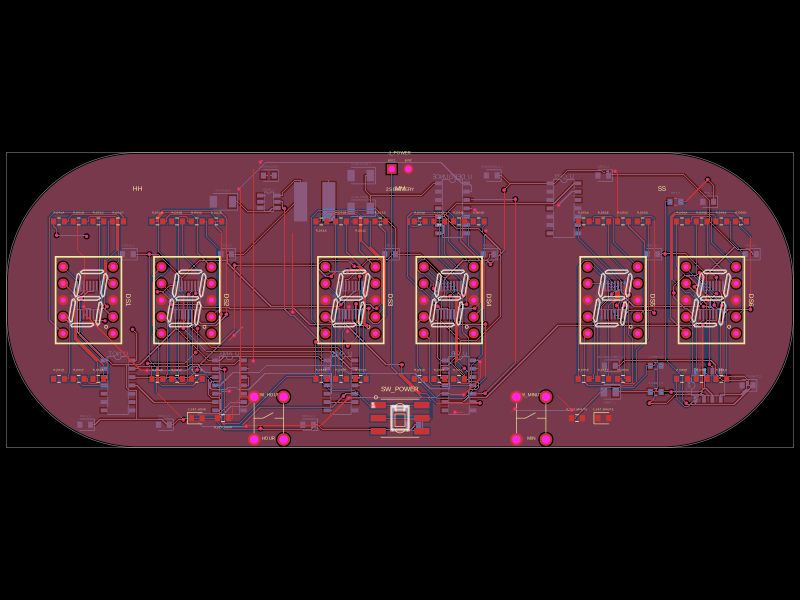 More from this authorgokul/new-clockThis code defines a PCB schematic with physical hardware components including switches, chips, resistors, capacitors, inductors, connectors, and visual annotations for a six-digit 12-hour digital clock circuit.
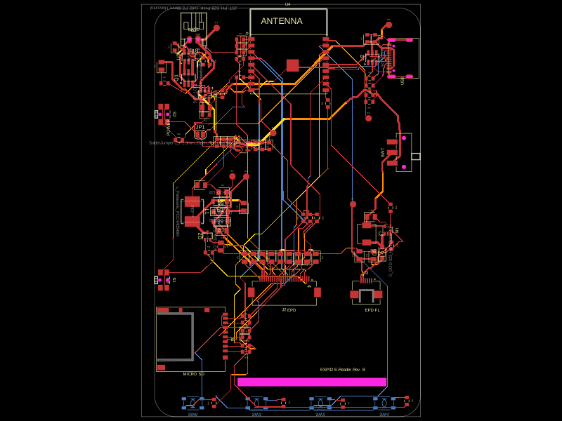 Similar packagerushabhcodes/ESP32-E-ReaderThis code defines the hardware layout and schematic connections for an ESP32-based e-reader device, including microcontroller, USB, display, power management, connectors, passives, switches, and associated PCB footprints, placements, and net connections.